Continue to Site

Welcome to EDAboard.com

Welcome to our site! EDAboard.com is an international Electronics Discussion Forum focused on EDA software, circuits, schematics, books, theory, papers, asic, pld, 8051, DSP, Network, RF, Analog Design, PCB, Service Manuals... and a whole lot more! To participate you need to register. Registration is free. Click here to register now.

Tuning the antenna to be conjugately matched to input impedance of the die

Status
Not open for further replies.

doenisz

Junior Member level 2
Joined
Sep 12, 2021
Messages
22
Helped
0
Reputation
0
Reaction score
0
Trophy points
1
Activity points
318
Hi guys,

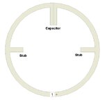
I am currently designing a circular loop antenna to be matched to the input impedance of the rectifier, at 3.5GHz. I did HFSS simulations to verify the impedance of the antenna plus the bondwires, and I used Cadence Post-Layout simulations to find the input impedance of the chip itself.

Basically, at 3.5GHz, the input impedance of the chip is like 0.7-j270, and the antenna+bondwire is 1.5+j270. For context, I'm following the methodology described here: https://ieeexplore.ieee.org/document/7435352

However, due to the other secondary effects I cannot control, they may not be matched at 3.5GHz and my chip does NOT have a control loop to adjust the resonance.

I can change some of the antenna geometrical parameters by cutting some traces etc. but I'll probably need a drilling machine. However, my antenna will be very close to the die (to reduce bondwire, transmission line and loss effects) so drilling machine may cause my wirebonds to fail.

I can always find the resonance frequency and then order new PCBs as a trial and error but wirebonding new dies to the new PCBs would cause a lot of time wasted and money too.

So, I would like to ask, in case I find that the resonance occurs at a higher or lower frequency that 3.5GHz, what can I do to tune this resonance? I also thought of using a varactor to tune the input reactance of the antenna but I was wondering how it would change the radiation efficiency?

Thanks.
 

What about the output impedance of the chip ? Is it very well controlled and fixed along a frequency band or it may show some/much deviation. You should ask this question first.
If there is no automatic mechanism, you will always loose or gain therefore you have to specify min. and typical values for a desired performance. Nothing is guaranteed in this world.

The good news is that the antenna impedance is very close to chip's input impedance so conjugate matching is almost there. A high valued coupling capacitor will terminate the matching.
Select a 0201 RF capacitor which does have a nominal value exceeding 3.5GHz.
 
Last edited:

What about the output impedance of the chip ? Is it very well controlled and fixed along a frequency band or it may show some/much deviation. You should ask this question first.
If there is no automatic mechanism, you will always loose or gain therefore you have to specify min. and typical values for a desired performance. Nothing is guaranteed in this world.
I don't know the output impedance because I just need to input impedance to know about the reactance, so that I can design an antenna to be conjugately matched to it, and then know the passive RLC boost on the input capacitance. What I mean by the input impedance is just the impedance seen looking into two RF inputs.
The good news is that the antenna impedance is very close to chip's input impedance so conjugate matching is almost there. A high valued coupling capacitor will terminate the matching.
Select a 0201 RF capacitor which does have a nominal value exceeding 3.5GHz.

Right but all of them are simulated values. I found the antenna impedance from HFSS simulations (bondwires considered), and chip's input impedance from Cadence Post-Layout simulations. So, it's not certain if they will be matched once I get the chip packaged.

Not sure if I fully understand the capacitor idea. Could you elaborate on what it does? Should I add it in series to the antenna and then (potentially) tune it during the operation to satisfy matching?
Best.
 

In that case, a strong matching is not necessary to my understanding.
Since the simulated impedances are close to reality, you can connect the IC directly to the antenna through a coupling capacitor. This capacitor will not serve to matching purpose but almost all IC have DC throughput that's why I said "connect a small capacitor"
The best way is to measure these impedances. If you're able to access to a Load Pull -even simple one- test bench, you can always match very well the IC to antenna. Theoretical values will you misguide.
Thank you, I will keep these in mind.
I have one more question. For my antenna to be low-loss, I am using Rogers 4350B substrate instead of FR4. I initially designed the substrate thickness to be 10 mils, but I was wondering if this would cause mechanical problems like being brittle. Should I make it 62mils like standard FR4?
Never used Rogers 4350B so I don't know how rigid of a material it is.
 

A lumped series capacitor will increase the resonant frequency of the loop, but at 3.5GHz will be hard to implement do to small dimensions of the loop.
You can design a printed capacitor to increase the resonant frequency, and/or a stub (or more) to decrease the resonant frequency.
 

Attachments

  • Loop.jpg
    Loop.jpg
    76.2 KB · Views: 95

Status
Not open for further replies.

Part and Inventory Search

Welcome to EDABoard.com

Sponsor

Back
Top