Continue to Site

Welcome to EDAboard.com

Welcome to our site! EDAboard.com is an international Electronics Discussion Forum focused on EDA software, circuits, schematics, books, theory, papers, asic, pld, 8051, DSP, Network, RF, Analog Design, PCB, Service Manuals... and a whole lot more! To participate you need to register. Registration is free. Click here to register now.

Transistor amplifier topology

Status
Not open for further replies.

miso156

Junior Member level 2
Joined
Jan 13, 2019
Messages
23
Helped
0
Reputation
0
Reaction score
0
Trophy points
1
Activity points
222
Hello,

I need to scale a DC voltage from range <1 - 2V> to range <1 - 7V>. I can use a single transistor amplifier circiut, becouse I need also inverse this signal.

But what I am interested is if have enough voltage level on input (more than 0.7) if is an R17 need, another words, if I can use an second circuit?

Any stability issue can occur or some another problem?

Thank you

Schema.jpg
 

Hi,

it looks like you are interested in amplifying an rectified AC signal. So as mentioned, you are interested in DC signals only.
Where is the output of your circuit? I assume it is it the BJT collector, as you mentioned the output signal is inverted.

- You could apply your rectification circuit at the output of your common emitter amplifier.
- AC couple your input by means of a capacitor, if your signal is really an AC signal.
- Bias your transistor by the resistive voltage divider as shown in the left circuit in your attached image.

Doing so, you have not to worry if your input signal is large enough to turn your BJT on.

greets
 

Hi,

A simple bjt won't work satisfactory.
There are Opamps, they can do it almost perfectly.

I'm not sure about your requirement.
* You say input range is <1 - 2V>. Does it mean that the lowest expectable input voltage is +1V and the highest expectable input voltage is +2V?
* ...similar with output voltage.
* You also say: becouse I need also inverse this signal.
Does this mean you need a second output signal?
An does it mean the output voltage should go from -1V to -7V?

A picture, a diagram, a formula tells more than a lot of words.

Klaus

Hi, thx,

-input is from +1 to +2 volts
-output is from +1 to +7 volts
-i need only the inverse signal
-the function should be linear, I am using C1518 gr3k transistor, seems its Hfe is constant.

I am asking about if the biasing is needed, if i have enough input voltage to drive Bjt directly?

- - - Updated - - -

Hi,

it looks like you are interested in amplifying an rectified AC signal. So as mentioned, you are interested in DC signals only.
Where is the output of your circuit? I assume it is it the BJT collector, as you mentioned the output signal is inverted.

- You could apply your rectification circuit at the output of your common emitter amplifier.
- AC couple your input by means of a capacitor, if your signal is really an AC signal.
- Bias your transistor by the resistive voltage divider as shown in the left circuit in your attached image.

Doing so, you have not to worry if your input signal is large enough to turn your BJT on.

greets

Hi,

its not a true AC signal, its a periadical dumped oscilation of RLC.

see figure:

Wave.png

However, i care about amplitude of positive part of wave, so i rectifie it and "store" the maximal value of amplitude to the capacitor. Then i need to scale it to wide range.

You mention about biasing. Is it really biasing needed if i have minimal value of input 1V? It can drive the Bjt even to saturation, no?

Thx
 

Hi,

Please understand that we only know what you show us. We don't have the background knowledge that you have.

So please explain:
* you say your input voltage range is +1V ... +2V, but the given diagran shows -0.7V .... +1.8V
* still unclear what "i need only the inverse signal" means.

Klaus
 

Hi,

Please understand that we only know what you show us. We don't have the background knowledge that you have.

So please explain:
* you say your input voltage range is +1V ... +2V, but the given diagran shows -0.7V .... +1.8V
* still unclear what "i need only the inverse signal" means.

Klaus

Ok,

this is the schematic:

Schematicc.png

its an serial RLC circuit fed by square wave. I measure the amplitude of R1 voltage (the maximal value). So i rectify it using diode D1 (it will cut the negative part of voltage) and filter it by capatitor C2.

Please dont take the waveform diagram accurate, its raw for now, and it also changes as i change the inductors.

Then i need to scale it in way:

+1V on input give +7V on output
+2V on input give +1V on output
 

Hi,

O.K. now it's much clearer.

I don't know what accuracy and precision you want..

Fir my tastet the value of C2 is much too high. It needs a lot of current to get charged. Then with R3 you get a too high time constant.
Thus you can't catch the peak voltage of R1.
With a smaller value of C2 you'd get a higher voltage at C2, since it's much closer to the peak voltage of R.
If you use a small schottky diode at D1

But then you also need a higher value of R4 .... not to discharge C2 too fast.
Currently you have a time constant of 64ms.
The higher the better.

Now to the end amplifier:
If you want an input range of 1V (+1V ... +2V) at C2 to become 6V (+7V ...+1V) at the output you need a gain of -6.
Usually you may estimate small signal voltage gain to be -R7/R5.
The base current will reduce this gain. For a lower base current you need a smaller collector (emitter) current.

For an almost ideal (one bjt) voltage amplifier the voltage at R5 is V_C2 - 0.55V --> 0.45V ... 1.45V
The voltage drop (at gain of 6) at R7 then would be 6 x V_R5 --> 2.7V ... 8.7V
With your R12 this is impossible.
Even if you omit R12 the output voltage then should be 8V - V_R7 --> impossible. (8V - 8.7V = negative)

Let's try to calculate backwards:
Output voltage 7V down to 1V needs a R7 voltage 8V - V_out of 1V up to 7V at R7.
This needs a R5 voltage of 0.67V .... 1.67V.

And here we see the biggest problem. You can't get 1V output voltage with V_R5 to be 1.67V.
The output voltage (at emitter) never can be lower than the R5 voltage (at collector)

And this is why I underlined the words "small signal" before. You are far away from small signal operation.
Your output signal is large ... indeed it is clipped.

--> I see no good solution to get your desired output signal with the current circuit.

You need some major modifications in your circuit. Less output voltage range, higher supply voltage...

Klaus

Thx, of course, I will not to try to do a impossible things.

I cannot increase a supply voltage, but i can change the output range (i choosed +1 to +7V very raw).

The condition is to make the output as wide as possible to prepare hight resolution for next circuits like comparator.

Can u pls caltulate the values of resistors to get maximum output range at 8V supply? (If can be 2 to 7 volts i dont care).

You can get rid of zener diode and R12, and supply the amplifier with 8V directly, its controlled with TL431 with 4m7 filter.

Regarding to precision, i will calibrate the device connected to the output, so the basic transistor amplifier should be enough. And of course, why to use precise OPAMPs if the input signal from R1 isnt linear function.

- - - Updated - - -

For now, i made it with this resistors, i got the output from 2.5V to 7.5V. I need to make down limit lower, 2.5V to lets say 1.5V.

How about stability issue, i notice some temperature dependence or something, the output changes from 2.54V to 2.59V after half an hour af running.

aaa.png
 

Hi,

my solution would be a tiny microcontroller with ADC.
I will
* generate the excitation signal (your astable multivibrator) with software adjustable frequency and timing, and extreme XTAL precision
* catch the signal with most precision (no rectifier needed, no peak detector needed), no delay, perfectly tracking the peak, easily to synchronize
* and it will perform additional functions (like your comparator) with perfect thresholds, adjustable, and adjustable hysteresis.
It will replace 17 parts of your schematic while increasing precision, speed, decreasing cost, no internal drifts, ...and providing most flexible adjustment per software.

But you will have your reason for your circuit.
*******

I won´t calculte the whole circuit for you.
But you may try:
* Omit D2 and R12 (to increase output voltage range)
* C2 = 470n (to get better track of peak)
* R4 = 160k (to keep your decay time constant)
* Q2 = BC547C (to reduce BOM, and adjust on gain and current)
* R5 = 2k (to decrease base current)
* R7 = 15k (to get expected gain)

No guarantee. Your simulation will show the results.
You are still in large signal area, htus expect unliearity.
And you will have thermal drifts, and drift with time, and there willl be bad PSRR...and there will be a lot of ripple (from one peak to next peak)
All this will decrease precision.

--> OPAMPS are much better. Microcontroller even better.
********

Precision = repeatability. It can´t be calibrated.
You may calibrate for accuracy.

Klaus

Thx,

-regarding to R4 = 160k, i need a time response to 100ms (i didnt mention :)), R4 must be lower
-regarding to R5 and R7, i need better output impedance , R5 = 2K2 is maximum alowable resistance, 4 comparators connected directly to collector will destroy the output voltage.
-i must put a voltage devider to input, because otherway i must connect high base resistor like 200k to base and than i dont get enough range on output. So devider decrease the capacitor voltage, and i can use a smaller base resistor like 22K - is it good aproach?

sss.png

Lets say the allowed precision is 100mV in 2 to 7V range.
 

output from 2.5V to 7.5V. I need to make down limit lower, 2.5V to lets say 1.5V.

Your output stage appears to be a class A amplifier. At no time does it provide low resistance to either supply rail, therefore you have reduced range of output voltage.

If you want larger output swings, then you want an amplifier that provides low resistance to one supply rail, while causing high resistance to the other supply rail. (And vice-versa.)
Possibly a half-bridge. This is contained in an op amp, by the way. The type with rail-to-rail output.

Hi, thank you,

I think class A is good for this purpose. The colector will supply very light circuit like this simple comparator:

ccc.png
 

Hi,

Lets say the allowed precision is 100mV in 2 to 7V range.
no way.
Even a 5°C ambient temperature shift will cause a higher output drift than 100mV. At least I guess so.

-regarding to R4 = 160k, i need a time response to 100ms (i didnt mention :)), R4 must be lower
Your schemtic of post#6 showed a capacitor of 4uF and a discharge resistor of 16k this gives a tau of 64ms.
The same I tried to get with my values.

is it good aproach?
I recognize that I don´t know enough about your requirements to answer this.

Klaus
 

Hi,

No guarantee. Your simulation will show the results.
You are still in large signal area, htus expect unliearity.
And you will have thermal drifts, and drift with time, and there willl be bad PSRR...and there will be a lot of ripple (from one peak to next peak)
All this will decrease precision.

--> OPAMPS are much better. Microcontroller even better.
********

Precision = repeatability. It can´t be calibrated.
You may calibrate for accuracy.

Klaus

When you mention large signal, if i look at datasheet of C1815, it has a constant Hfe in whole range of Ic. Shouldnt be linearity good?


qqq.png
 

Hi,

indeed it´s better than I expected.

Klaus
 

I think class A is good for this purpose.

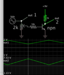
Aha... Okay then, it looks like you're on the right track. Here's my similar schematic of an NPN amplifier.

NPN amplifies signal 1-2v and inverts direction 9V supply.png

Incoming signal is 1 to 2V. Output covers the range you request. Linear response is possible since your signal is above 0.6V bias threshold.

If necessary you can install resistors where they exist in your schematic.
 

Status
Not open for further replies.

Similar threads

Part and Inventory Search

Welcome to EDABoard.com

Sponsor

Back
Top