Continue to Site

Welcome to EDAboard.com

Welcome to our site! EDAboard.com is an international Electronics Discussion Forum focused on EDA software, circuits, schematics, books, theory, papers, asic, pld, 8051, DSP, Network, RF, Analog Design, PCB, Service Manuals... and a whole lot more! To participate you need to register. Registration is free. Click here to register now.

[SOLVED] Transformerless power supply issue

Status
Not open for further replies.

Mithun_K_Das

Advanced Member level 3
Joined
Apr 24, 2010
Messages
899
Helped
24
Reputation
48
Reaction score
26
Trophy points
1,318
Location
Dhaka, Bangladesh, Bangladesh
Activity points
8,252
There are different types of Transformerless power supply designs. Most easy and common one we use in small designs is:

1709455138068.png


Besides this design, we also use this design,


1709455386623.png


These circuits are very simple and have the minimum components. But the problem is, the zener diode frequently gets burnt and if the voltage variation is over 20V, then output goes low in case of low input and in case of high input, the zener becomes hot, and at a time it gets burnt.

To prevent this, usually, a transistor is usually used with zener and resistors. But in that case, the output voltage drops as well as cost & component increases.

There are ICs like Viper12A/22A but those also increase component number as well as cost. In this situation, what else can be done so that the zener lasts longer and also the circuit's overall cost does not increase significantly?
--- Updated ---

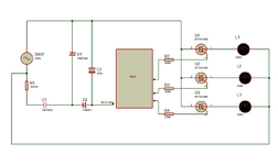
Note that the load we are driving with this power supply is an MCU, an IR sensor, and some TRIACs. Overall max consumption is 100mA @5V
 

It makes little sense to discuss "transformerless supply" topologies without considering if and how the load, e.g. triac switch is connected to mains. If it is, bridge rectifier topology can't be used.
 

I agree with FvM.

* specify the input min, max voltage, frequency ...
* specify the output: min, max voltage, min, max current.
* specify your additional requirements, like: volume, cost, power dissipation, casing, ....

.. and we can discuss about it.

*****
Just a bit of analyzing your second schematic:
110V AC input and a 10k ... limits the current to 11mA. What´s the use of the 250mA fuse. It´s nonsense in my eyes.
110V AC input and a 10k ... limits the power dissipation to 1.2W.

110V AC and 10k + 0.22uF (assumed 60Hz = 12k) gives 15k6 ..and thus limits the current to 7mA (btw: this combination makes no sense in my eyes. Contact and blame the person who designed it for bad working)
7mA on a zener with 5.1V give a power dissipation of tiny 36mW ....(whil even the small ones are 500mW rated)
If now the diode becomes hot - as you say - there need to be at least two other parts defective!

Physically and mathematically your description can´t match the given circuit. So please don´t fool us.
--> give matching informations with good descriptions ... then we can help you.

Also you are free to use circuit simulation tools. There are easy to use free to download ones.

Klaus
 

Not sure why your Zener is burning out, unless its junction T is being aggravated
by the 10W 2K ohm R, which happens to be the hottest device in the design. Also
notice trying to take ~5 ma in that design (R2) zener never achieves its design V.

And if you are trying to gen 5.0 V out then Vz should be 5.6V to account for loss of
diode drop in D2.

1709482043676.png


Regards, Dana.
 
Last edited:

1710258500210.png

Dear supurior,
Thanks for finding it nonsense as I can not expose everything directly due to NDA at the first message. But I've to do some now. Here is the circuit diagram we use. Of cource kindly don't find mistakes drawing the TRIAC connections and where the MCU VDD connected which is not our focus point, MCU VDD is directly connected to the Live line. And we have been using this circuit diagram for almost 12yrs+ in similar designs. All of them have one common issue is the burning the zener diodes over time.

So my question was little bit indirect in the begining. But all parameters are like this:
Input: 160V ~240V AC, 50Hz.
Loads: 100Wx3 to the TRIACs
MCU consumption: Never measured.
TRIAC Gate consumption: ~15mA each
MCU VDD: 5V

A sensor is connected which consumes 2mA max

Note: All the 3 loads are not running at a time. Any two is running at a time.

I hope now it won't be a nonsense idea to get the information. Thanks again. Sometimes I feel "its better to solve any issue myself rather than asking anyone" while I post anything on this platform.

I agree with FvM.

* specify the input min, max voltage, frequency ...
* specify the output: min, max voltage, min, max current.
* specify your additional requirements, like: volume, cost, power dissipation, casing, ....

.. and we can discuss about it.

*****
Just a bit of analyzing your second schematic:
110V AC input and a 10k ... limits the current to 11mA. What´s the use of the 250mA fuse. It´s nonsense in my eyes.
110V AC input and a 10k ... limits the power dissipation to 1.2W.

110V AC and 10k + 0.22uF (assumed 60Hz = 12k) gives 15k6 ..and thus limits the current to 7mA (btw: this combination makes no sense in my eyes. Contact and blame the person who designed it for bad working)
7mA on a zener with 5.1V give a power dissipation of tiny 36mW ....(whil even the small ones are 500mW rated)
If now the diode becomes hot - as you say - there need to be at least two other parts defective!

Physically and mathematically your description can´t match the given circuit. So please don´t fool us.
--> give matching informations with good descriptions ... then we can help you.

Also you are free to use circuit simulation tools. There are easy to use free to download ones.

Klaus
 

Attachments

  • 1710258036124.png
    1710258036124.png
    43.2 KB · Views: 44

Hi,

nobody asks for confidential informations.
No one asks for a detailed circuit.

You ask for a power supply, and for this power supply one neesds specifications like voltages and current. Nothing fancy, just basic informations. Nothing that is protected by an NDA.
If you wanted to buy a power supply you need to know the same specifications.

No one said it is nonsens to discuss a schematic.
The only time "nonsense" came up was with a 250mA fuse on a node which draws not more than 11mA worst case.

****
This is a new power supply circuit.
Why do you post three different circuits?
Which one is the circuit you really use? This on from post#6? Then a destroyed zener makes sense.
But the zener won´t burn with the circuits from post#1. I commented on the circuits of post#1, because this was the given infromation. We did not know that there is a third circuit.

Klaus
 

In simulating these capacitive drop supplies I've found it necessary to find a suitable value for R1, because without it the entire circuit gets jolted by strong startup surge. For this reason R1 should be a substantial ohm value. Its value is a tradeoff because it creates its voltage drop in addition to the capacitor's voltage drop.

So R1 needs sufficient power (Watt) rating too. You might as well make full utilization of R1's Watt rating and give it more burden. That way it takes stress off the capacitor. And reduces startup surge to the entire circuit.

In earlier years we planned on using a transformer. 6V 150mA type were readily available cheap. Since prices rose many designers have transitioned to capacitive drop. It's an irresistible alternative. However the price is greater effort needed in designing component values.
 

Hi Dana.

good job.
If you can spend the time then I think it´s a good idea also to show what happens when the power supply is switched ON close to sine_peak.
(obviously the "unhealty" timing for the zener, like Brad mentioned.)

If you have even more time then you could do the same with the circuits of post#1.
Just to show the OP that the circuits differ alot in this behaviour.

In worst case this is just a couple of mA of zener current in the circuits of post#1 while it is maybe 1000 times (!!!) higher with the circuit of post#6.
The OP seems not to be aware that with the schematic of post#1 it is almost impossible to destroy a zener, while it is rather likely to destroy a zener with circuit of post#6.

Klaus
 

Hi,

yes, blame it on us, that we don´t have a crystal ball to see that
* you use 220V instead of your shown 110V
* you use 1R instead of the shown 2000R or 10000R shown in your post.

Sorry for wasting your time with my math and asking for valid informations ... it won´t happen again!

Klaus
 

In simulating these capacitive drop supplies I've found it necessary to find a suitable value for R1, because without it the entire circuit gets jolted by strong startup surge. For this reason R1 should be a substantial ohm value. Its value is a tradeoff because it creates its voltage drop in addition to the capacitor's voltage drop.

So R1 needs sufficient power (Watt) rating too. You might as well make full utilization of R1's Watt rating and give it more burden. That way it takes stress off the capacitor. And reduces startup surge to the entire circuit.

In earlier years we planned on using a transformer. 6V 150mA type were readily available cheap. Since prices rose many designers have transitioned to capacitive drop. It's an irresistible alternative. However the price is greater effort needed in designing component values.
The transformer is ok. but size is the issue. As these types of circuits need to fit in very small enclosers, everything is placed in so a way to fit all in. Also, price is another issue too. so a capacitor is the best choice. If we use a higher R1 value, the resistor loss becomes high and it starts dissipating heat. Sometimes this heat becomes a smoky level/smell. Which is not safe. So year after year of testing, we found an optimum value of 1R. But the zener diode issue is not recovered in any way.

Have been using the transistor + zener combination but this drops voltage and the transistor also becomes hot after some time. [this is still under testing]
 

Here is the circuit diagram we use. Of cource kindly don't find mistakes drawing the TRIAC connections and where the MCU VDD connected which is not our focus point, MCU VDD is directly connected to the Live line. And we have been using this circuit diagram for almost 12yrs+ in similar designs. All of them have one common issue is the burning the zener diodes over time.
12 years of using this type of circuits, why don't you draw triac polarity correctly?

According to my math the circuit supplies 32 mA DC with 230 VAC 50 Hz, capacitor and grid voltage tolerances should be considered, thus 25 mA maximal load is a reasonable figure.

The 1 ohm series resistor is built-in self destruction in my view. The resistor must be dimensioned so that grid with high harmonic voltage content and plug-in surges don't cause too high currents. There are many devices on the market using capacitive voltage drop, e.g. automatic light switches. Enough stuff to study reasonable dimensioning.
Intentionally man!

That is not the main focus of the issue. I hope you are mature enough to understand. Thank you!

according to calculation, many things go a different way from practical.
 

O.k., you are intentionally showing an "obfuscated" schematic. Then there's nothing to discuss about possible reason of failure. Happy developing!
 
Status
Not open for further replies.

Similar threads

Part and Inventory Search

Welcome to EDABoard.com

Sponsor

Back
Top