Continue to Site

Welcome to EDAboard.com

Welcome to our site! EDAboard.com is an international Electronics Discussion Forum focused on EDA software, circuits, schematics, books, theory, papers, asic, pld, 8051, DSP, Network, RF, Analog Design, PCB, Service Manuals... and a whole lot more! To participate you need to register. Registration is free. Click here to register now.

TPS54331-DC2DC Voltage Output

tiwari.sachin

Full Member level 6
Joined
Aug 1, 2009
Messages
341
Helped
3
Reputation
6
Reaction score
3
Trophy points
1,298
Location
India
Activity points
4,449
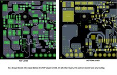
I have designed a DC to DC that has input of 12 to 18V and output at 8.5V.

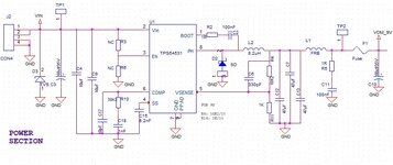
Following is the schematic used

SCH.jpg


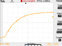
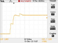
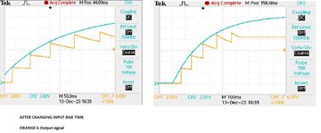
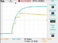
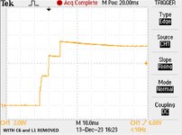
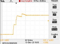
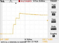
I am getting the desired result but when I measure the output, I am getting the following result

GRAPH.jpg


The output rise isnt smooth as expected.

What could be causing this or am I doing something wrong on the schematic side.

Regards

Sachin
 
Hi,

Please use the [insert Image] button or use [Ctrl]+[P] to upload pictures.

What does "isn´t smoot as expected". --> please tell us what you expect. Draw a sketch.

Switch mode power supplies need careful PCB layout design to operate properly. -->Show us your PCB layout.

Klaus
 
Hi,

I was expecting the output curve for the given schematic as below
--- Updated ---

Schmatic and Output curve that I am getting is attached.
 

Attachments

  • OUTPUT EXPECTED.png
    OUTPUT EXPECTED.png
    268.8 KB · Views: 53
  • GRAPH.jpg
    GRAPH.jpg
    67.5 KB · Views: 55
  • SCH.jpg
    SCH.jpg
    115.8 KB · Views: 52
Hi,

if you want a start upt ime of more than 20ms as shown in the "output_expected" picture, then use Formula 3 of the datasheet.

I expect the correct SS capaciotr will bring some benefit.
But the start up ripple most probably is caused by a bad layout ...
Also critical is capacitor, inductor, diode selection. We don´t see what exact parts you did use. Hopefully you followed the datasheet guide.

If you want me to give more detailed feedback: Provide the missing informations.

Klaus
 
Hello,

I have attached the various waveforms I tried and also the routing of DC2DC Section (Bottom is mirrored so that understanding of routing can be easy in image)
--- Updated ---

I expect the correct SS capaciotr will bring some benefit.

Signal shown as "Expected Signal" is only for reference. I am ok with the rise time of output I am getting
 

Attachments

  • INPUT & OUTPUT SIGNALS AFTER CHANGING INPUT RISE TIME.jpg
    INPUT & OUTPUT SIGNALS AFTER CHANGING INPUT RISE TIME.jpg
    180.1 KB · Views: 38
  • INPUT & OUTPUT SIGNALS.jpg
    INPUT & OUTPUT SIGNALS.jpg
    86.8 KB · Views: 35
  • WITH C6 AND L1 REMOVED.jpg
    WITH C6 AND L1 REMOVED.jpg
    81.8 KB · Views: 40
  • WITH C6 REMOVED.jpg
    WITH C6 REMOVED.jpg
    72.8 KB · Views: 41
  • WITH C6, L1 REMOVED, R2 SHORTED.jpg
    WITH C6, L1 REMOVED, R2 SHORTED.jpg
    80.6 KB · Views: 40
  • ROUTING_TOP & BOT.jpg
    ROUTING_TOP & BOT.jpg
    437.5 KB · Views: 44
I wonder if the DC/DC is loaded with actual output current in your test. For me it looks like a badly compensated control loop (gain to high).
 
HI,

removing C6 is counter productive.

I´m talking about the SS capacitor. C15. --> don´t remove it. Calculate the correct value. I expect a bigger value.

Btw: If you do multiple scope pictures: please keep horizontal and vertical setup .. for them to be compared more easy.

Klaus
 

LaTeX Commands Quick-Menu:

Similar threads

Part and Inventory Search

Welcome to EDABoard.com

Sponsor

Back
Top