Continue to Site

Welcome to EDAboard.com

Welcome to our site! EDAboard.com is an international Electronics Discussion Forum focused on EDA software, circuits, schematics, books, theory, papers, asic, pld, 8051, DSP, Network, RF, Analog Design, PCB, Service Manuals... and a whole lot more! To participate you need to register. Registration is free. Click here to register now.

TL494 DCDC converter wide range input issues

Zac1

Member level 1
Joined
Mar 17, 2024
Messages
36
Helped
0
Reputation
0
Reaction score
1
Trophy points
8
Activity points
365
With a help of few people I managed to design fairly wide range DCDC converter using TL494

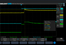
I confirmed it works in range of 30-190V DC
Has fairly stable 12V output with ~40mV peak to peak noise
Can deliver up to 3A.

However it has one fatal flaw that haunts me in my dreams. It kills mosfet Q5 and diode D2 if you suddenly apply 160V+ (high dV/dt)
It does work properly if slowly raising voltage across 40-190V. Also works up until 140V (sudden turn on).

I have managed to capture the problematic moment on thermal camera


Basically there is a full short on Q5 and D2 for a moment, then fuse pops and both components have dead short. I have tried to remedy this situation with help of PNP clamp (Q1) but it doesn't do much. I am out of ideas how to fix this... perhaps the driver is at fault? Or maybe diode is too slow?


1710670474787.png
 
Solution
it needs to be speeded up / higher gain - until it becomes unstable - then back off a bit
I think this can be done after I order PCB, right now i need to order asap to have something to play with.

both soft start and/or dc gain can be adjusted with just cap/resistor values.


Why is the switcher driving high current into D3 even in steady state although the nominal output voltage is said to be 12V? There seems to be a problem with voltage feedback operation point.
I am sorry, i did not understand question? D3 after startup should see a max of 52micro amps.


As already stated, soft start time constant should be much higher, I'd test with 5 or 10 uF C5.
Will do, right now i think i have complete PCB that should...
OCP is high speed so that seems to suit your design. You can choose from many high or low side 50 mV current sensor designs to disable the drivers and clamp the flyback with a diode and latch off and display a fault LED.
 
Last edited:
I have made version 3 of this circuit and I have some good and bad news.

Bad:
First of all Zener diode on the output dies no matter what at VIN > 130V.

Good:
Even if zener dies, both Mosfet Q5 and diode D2 survives
Without zener diode this circuit is able to withstand sudden turn on at 184V

Meh:
It will not work if there is no load on the output, at least equivalent of 1k resistor so 12mA or 0.144W
Its not that big of a deal but something i have to keep in mind.


It dies probably because there is quite big overshoot at start:
1712452965720.png


It ramps up to 21.6V and stabilizes at 11.9 after ~50ms, even with soft start and dead time limit.
New startup circuit is powerful enough to drive entire DCDC converter by itself, but I have managed to fry depletion mode nfet (Q2) once and I cannot reproduce it.

That 21V gets me a little worried so the question is, should I just try with 16V Zener ex 5-10W to soak that initial spike?
 
At high Vin, very little pwm is needed for plenty of output, so the soft start must be quite slow as a consequence,

what was the previous zener power rating ? a 16V 5W zener - or 2 in // may be a solution - but the currents will obviously be high and may saturate your choke - a 0.1 ohm R can be used to see the output current at start.
--- Updated ---

It does appear your feedback loop could be faster - this would really reduce the overshoot !

--- Updated ---

try C1 = 22n, R6 = 4k7, R14 = 39k, according to the ckt in post #1

Also a 1k load to allow a start is no great hard ship
 
Last edited:
what was the previous zener power rating ?
I have tried 13V 3W zener and 15V 1W zener, both died at same voltage levels.


I had some bedtime thoughts to debug it more in depth and here is what I came up with, measuring overshoot at different VIN levels. Starting up from 43V
Legend:
yellow - main mosfet gate (just sanity check if it gets signal from TL494 and driver)
green - output (12V out)
blue - input (VIN)

1712488949313.png


So results are:
1. VIN 43V, overshoot 19.5V
2. VIN 57V, overshoot 19.7V
3. VIN 71V, overshoot 20.7V
4. VIN 83V, overshoot 21.2V
5. VIN 99V, overshoot 21.3V
6. VIN 113V, overshoot 21.5V
7. VIN 125V, overshoot 21.7V
8. VIN 137V, overshoot 22.1V
9. VIN 145V - driver died, depletion fet may have partially died (CPC3980)

So while I wanted to try changing feedback loop like you suggested, it will have to wait until i get replacement for it.

EDIT:

Seems like driver died IR2181 but depletion mode mosfet could have been hurt as well. Without anything else startup circuit is providing 10V. I took a moment to record how startup circuit starts in isolation (without TL494 and without driver):
1712491275991.png
 
Last edited:
Do you understand why you were getting a power surge yet?
It seems to me the HO driver is on all the time and the PWM is late in getting started until it is too late then you have massive overshoot.

Something fundamentally wrong here.
 
It seems to me the HO driver is on all the time and the PWM is late in getting started until it is too late then you have massive overshoot.
Driver is definitely not ON all the time, if you take a look at first pic here is what is happening.
for first 10ms absolutely nothing, then during next 10ms driver is outputting PWM on mos gate but slope is too steep and TL494 doesn't get change to react fast enough.

Which can be probably fixed with 2 things. speeding up control loop, slowing down raising time, perhaps by reducing inductor size. I will try values suggested by easy peasy when I get replacement parts.
 
You can see all the way through the feedback loop is way too slow, the addition of a small ckt to shut down the TL494 pwm at 13V

out would be a useful thing to have here. Op-amp 2 in the chip could easily be used to do this.
 
Last edited:
p.s. if you zoom in properly on the applied step for Vin ( light blue in the above images ) - you will see an appreciable overshoot ! - this is why 200V parts don't cut the mustard.
 
Components replaced, going again, only on power supply at 55V, no zener on the output.

First control (no changes to pcb):

1712676590467.png


try C1 = 22n, R6 = 4k7, R14 = 39k, according to the ckt in post #1
Now second test with those values. Whole dcdc bootloops

1712677506097.png


Control PCB but with C20 = 22uF (biggest longest softstart possible)

1712680058734.png
 
Last edited:
We can't easily tell what is what in the pictures, blue = pwm ? what are the others ? we can't see the graticles or easily derive the volts either - I assume the yellow is Vout ? & green is Vin - the feedback loop is still way too slow

What does " boot loops " mean ?

--- Updated ---


( try C1 = 22n, R6 = 4k7, R14 = 39k, according to the ckt in post #1 )

now try 10n for C1, then 4n7 !
--- Updated ---

In case you TLDR, I retype:

a good idea to shut down the TL494 pwm at 13V out. Op-amp 2 in the chip could easily be used to do this.

--- Updated ---

What value is R23 - the soft start ? DTC resistor ? can you make it larger for a longer soft start ?

as the pair set the max PWM you have to increase the upper resistor in proportion to maintain the same max PWM ~ 40%

--- Updated ---

Also - for a more active soft start - try the following:

R20 -> 100k, R21 -> 27k, then put 100nF and 100k in series across R20, this will feed current into the volt sense pin as the Vout comes up

and give a softer start ( for nearly 10mS )
 
Last edited:

    Zac1

    Points: 2
    Helpful Answer Positive Rating
WE can't tell what is what in the pictures, blue = pwm ? what are the others ? we can't see the graticles or easily derive the volts either
Ah sorry, yellow = output
Green = input
blue = mosfet gate vs gnd

What does " boot loops " mean ?
repeatedly turns on and off.

I have also tried one more thing that came to my mind. clamping just the "STARTUP" node with zener and limiting current with resistor:

D5 is currently replaced with 1k resistor

1712703438469.png


As a result, there is now significantly less overshoot (15.8V) on the output (this is not the same node as "STARTUP")
1712703504924.png


thermal cam also shows a lot less current being drawn when turned on:
https://cdn.discordapp.com/attachme...a725efe73cbcb1d868644c8bdf4b6ded800c8055fc5d&
 
this is only at 50V Vin right ?
Yes but problem was visible on all voltage ranges, it just so happened that above certain threshold driver or Zener (D5) died. Removing the D5 revealed nature of the problem.

Today i will test this new idea against higher voltages.
 
We already knew the problem - too much power overshoot at start up causing zener heating and quite likely inductor saturation.
I may be wrong on this one but i don't think this is the real issue. Or to be precise, why that overshoot was caused.

From what scope tells me, it has evertything to do with initial jump of chip supply voltage. I am not sure how to explain it properly but i will try:

at the startup both driver and TL494/driver get only ~10V. So it adjusts all its parameters according to it. But at some point, when output reaches >10V everything starts to change, voltage on mosfet gate raises, more current is being dumped and TL494 cannot keep up.

Now, new set of test reveals

1. VIN = 39V, VOUT overshoot = 15.4V
2. VIN = 49V, VOUT overshoot = 16.8V
3. VIN = 63V, VOUT overshoot = 17.6V
4. VIN = 80V, VOUT overshoot = 18.4V
5. VIN = 93V, VOUT overshoot = 19.2V
6. VIN = 118V, VOUT overshoot = 20.0V
7. VIN = 127V, VOUT overshoot = 20.8V
8. VIN = 147V, VOUT overshoot = 21.2V
9. VIN = 159V, VOUT overshoot = 22.4V
10. VIN = 165V, VOUT overshoot = 23.2V
11. VIN = 173V, VOUT overshoot = 23.2V
12. VIN = 183V, VOUT overshoot = 24.0V
13. VIN = 187V, VOUT overshoot = 24.0V

Legend:
yellow = output (12V node)
green = TL494 output, driver input
blue = VIN

93V:
1712738583801.png


147V:
1712738949217.png


187V:
1712739594375.png


Now, while the overshoot is problem and i would probably need to speed up TL494, at least zener on the startup node prevents thermal issues:

This was 187V, 3x fast turn on/offs with little waiting in between:

https://cdn.discordapp.com/attachme...0b94b32ac2fe9e0729c5c895ac8e7b338aa7b7237173&
 
Hi,

to be honest I did not dive deep into the datasheet nor into your circuit.

As others said the regulation loop seems to be is too slow.

Just an idea:
This may be because of start_up regulation offset the "integrator C1" becomes charged. (Referring to circuit of post#1)
.. and it needs time to discharge it when in regulation. (too much time)

Maybe you could use a diode for "fast discharge" of C1 on output_overvoltage.
Maybe a diode across R6 or R14.

Scope pictures of the involved nodes of the regulation loop could clarify this.

Klaus
 
I have added D component do PI making it PID (just a cap 100nF parallel to R14) and that managed to reduce overshoot significantly.

160V with 16V zener, no flare (meaning there isn't much energy dissipated on it):
blue = VIN
green = STARTUP node
yellow = VOUT

1712795308965.png


160V thermal boot:
https://cdn.discordapp.com/attachme...5d97b3b1f0b33177480f2812af868cadc23929f51eec&

190V thermal boot looks pretty much the same, and this is how scope looks like at 191V zoomed in:
1712795767803.png


I will order more values of capacitors between 100n->1u to test how it behaves but i believe i have my solution.
 

Attachments

  • 1712795646304.png
    1712795646304.png
    148.4 KB · Views: 21
Please don't take this the wrong way - but looking at the heat signature in the zener - is about as opposite as you can get to designing a power supply properly

you know nothing about the peak currents in the inductor - so you can't tell if it saturates or not - this is kind of a big deal. It can be easily measured and seen on a scope.

The engineering approach is to observe the Vout & error amp output at start up, and adjust the control loop accordingly such that it is fast enough ( and with just enough gain ) to keep the overshoot to a couple of volts max at startup & max Vin - also with the speed-up circuit on the Vsense

The trouble with not having a good knowledge or circuit behaviour - is that some thing small can change later on and break the expected behaviour in a bad way.

For example - if some one changes the inductor later on - and the new one saturates at a slightly lower current - you will be back to blow ups at switch on.


--- Updated ---

" I may be wrong on this one but i don't think this is the real issue. Or to be precise, why that overshoot was caused. "

you are correct in the first part
--- Updated ---

p.s. the gate drive chip only starts to operate when it gets 10V on its supply - this is why you don't see much happening until this 10V level is reached,

if you had read the data sheet you would have been aware of this.
 
Last edited:
Hi,

I totally agree with EasyPeasy.
If the gate driver starts delayed (caused by slowly rising VCC), then
* the internal soft start can´t work properly (I mean it works, but in the time when the driver does not yet work. So it´s useless)
* the integrator in feedback loop will be charged .. causing an overshot (because it needs output_overvoltage to discharge)

My recommendation is to build an external soft start, by ramping up VRef (1) slowly.
(I´m referring to schematic of post#1)
There are several ways:
One of the simplest is to connect a 220uF across R10.
This causes the feedback_VRef to ramp up slowly. Thus the voltage regulation setpoint is not yet at 100% when the driver starts to work

Other options:
* speed up VCC rise at power up (reduing capacitors, adding speed up capacitors, increasing current...)
* adding power supply monitors that shut down VRef (1) when VCC is not yet completely up
* or limit integrator_C voltage by adding diodes to avoid runaway

(1): the Ref voltage for the feedback loop

Analyzing the feedback loop signals would proof the caus of fail as well as workaround.

Klaus
 
p.s. the gate drive chip only starts to operate when it gets 10V on its supply - this is why you don't see much happening until this 10V level is reached,

if you had read the data sheet you would have been aware of this.
10V is reached pretty much immediately. I have tested this circuit many many many times. I don't see much happening for first 10-80ms simply because of soft start. Previous version starts immediately. And it was bad, sof start already helps a lot.
1712827804145.png


Another difference between pcb V1 and V2 is the power of startup circuit. If i desolder D6, V2 will continue to operate, both TL494 and driver will operate JUST powered by startup circuit. Depletion fet will get hot but it will work. Already tested that. As a result, what's on the output doesn't matter at all (i mean TL494 will try hardest to keep up).

Please don't take this the wrong way - but looking at the heat signature in the zener - is about as opposite as you can get to designing a power supply properly
What heat signature? I specifically marked zener with P0 marker, I hope you don't mean that 1k resistor that is right next to it? Because zener itself doesn't heat up, maybe jumps 1C then gets heated by resistor.

The engineering approach is to observe the Vout & error amp output at start up, and adjust the control loop accordingly such that it is fast enough ( and with just enough gain ) to keep the overshoot to a couple of volts max at startup & max Vin - also with the speed-up circuit on the Vsense
I have been observing FB pin while playing with cap, thing is, calculated values point to value ~22nF -> ~600nF, unfortunately i do not have many values in that range so I had to order more. Which means I will continue to try to dampen it. But 100nF already did good job.


* the internal soft start can´t work properly (I mean it works, but in the time when the driver does not yet work. So it´s useless)
That is not what is happening. I can't stress that enough but startup circuit built on depletion fet works marvelously. It delivers enough power for entire circuit for unlimited amount of time (at least until it reaches high temp and die but that would take at least dozens of minutes). If you really want to see it i can disconnect D6 and show you guys.

One of the simplest is to connect a 220uF across R10.
This causes the feedback_VRef to ramp up slowly. Thus the voltage regulation setpoint is not yet at 100% when the driver starts to work
Thank you for that suggestion, this is certainly something i can try! Once i get capacitors I ordered.
* adding power supply monitors that shut down VRef (1) when VCC is not yet completely up
I thought about that but I am kind of running out of space on PCB.

As it stands right now, current test version works pretty well. I tested like 50 startups on various voltages between 120-190V with minimal heat flare. I have also prepared a photo with explanation of current PCB. Nerevmind the mess and flux, I did so many tests on it i couldn't bother to clean up.

I apologize in advance for any confusion I may have caused:
1712829926483.png
 

LaTeX Commands Quick-Menu:

Similar threads

Part and Inventory Search

Welcome to EDABoard.com

Sponsor

Back
Top