Continue to Site

Welcome to EDAboard.com

Welcome to our site! EDAboard.com is an international Electronics Discussion Forum focused on EDA software, circuits, schematics, books, theory, papers, asic, pld, 8051, DSP, Network, RF, Analog Design, PCB, Service Manuals... and a whole lot more! To participate you need to register. Registration is free. Click here to register now.

The impact of the shrinking process window and its effects on parametric yield.

Status
Not open for further replies.

ameed

Advanced Member level 4
Joined
Jun 28, 2007
Messages
106
Helped
6
Reputation
12
Reaction score
1
Trophy points
1,298
Location
INDIA
Activity points
1,931
hi all,

With the Moore’s law defining the emerging sub nano technology nodes like 45nm and
32nm, it is high time that the designers who were till now typically concerned about
performance parameters like speed and power also take into consideration the impact of
the shrinking process window and its effects on parametric yield.
Effect of Shrinking Geometries

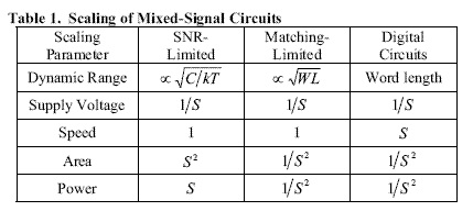
what effect can be getting releted to speed and power:?:
 

layout design

see the Pic

Added after 28 seconds:

https://obrazki.elektroda.pl/70_1187869578.gif

Added after 1 minutes:

70_1187869578.gif
 

layout design

ameed,

I think if technology is shrinking then voltage level also going down. on chip area will take less there DRC rules are changing. Power will increase. I don't know @ speed. you should take care @ electro migration. Channel length will decrease then speed will increase. Velocity saturation effect will come there.
.......................................................................
 

Re: layout design

supply voltage will decrease, speed will be faster, power consumption maybe larger or smaller.
 

Re: layout design

hi FRNDZ,
as the device scalling is shrinked down,power consumtion will get increase due to leakage power dissipations,speed also increases as the device size(length decreases),
electromigration propbems will take into effect,shortchannel effect(velocity saturation) effect also there.
 

Re: layout design

as device scales down SiO2 layer thickness decreases which results in leakage of current, to rectify this Hi-K material is used. Speed increases as frequency increases when technology scales down.
 

Status
Not open for further replies.

Part and Inventory Search

Welcome to EDABoard.com

Sponsor

Back
Top