Continue to Site

Welcome to EDAboard.com

Welcome to our site! EDAboard.com is an international Electronics Discussion Forum focused on EDA software, circuits, schematics, books, theory, papers, asic, pld, 8051, DSP, Network, RF, Analog Design, PCB, Service Manuals... and a whole lot more! To participate you need to register. Registration is free. Click here to register now.

the difference of application and layout between isolation nmos and normal nmos ?

Status
Not open for further replies.

mpig09

Full Member level 4
Joined
Aug 26, 2005
Messages
232
Helped
8
Reputation
16
Reaction score
2
Trophy points
1,298
Location
Taipei
Activity points
2,810
Hi all:

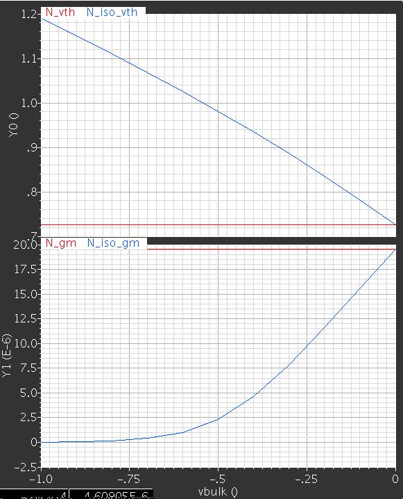
There are two nmos models in the spice model : isolation nmos and normal nmos.
I simulate the i-v curve, and the result shows the curve are the same with isolation nmos and normal nmos.

Does anyone know the difference of application and layout between isolation nmos and normal nmos ?


Thanks for your view and reply.
mpig
 

In a standard CMOS process with p- substrate, the bulk of a normal nmos is automatically connected to the substrate: it is the substrate - which has the most negative potential of the circuit (GND). If an nmos is needed whose bulk should not be connected to GND, an isolated nmos is needed, whose bulk can be connected to some higher potential, e.g. to its source of a stacked nmos, by this eliminating the automatic positive source-to-bulk voltage which would change its threshold voltage and transconductance.

Again, in a standard CMOS process with p- substrate, such an isolated nmos has to reside in a separate pwell which is totally immersed in an nwell. For this, a twin well or triple well process is needed, s. e.g. this image:

isolated_NMOSFET.png

So it's no surprise that the i-v-characteristics of both the normal and isolated nmos are identical if both have their sources connected to their bulks.
 
Hi erikl:

Very thanks for your reply.
The reply let me more clear the iso-nmos.

I check the layout and re-simulate the gm and vth of iso-NMOS and nor-NMOS.

simulation:
The pic shows the simulation result:
N_ is a normal NMOS and vsb=0
N_iso is a iso-NMOS and sweep vsb=-1V ~ 0V


I hope erikl's reply and my simulation result will let us
to know iso-NMOS more clearly.

mpig
 

Status
Not open for further replies.

Part and Inventory Search

Welcome to EDABoard.com

Sponsor

Back
Top