Continue to Site

Welcome to EDAboard.com

Welcome to our site! EDAboard.com is an international Electronics Discussion Forum focused on EDA software, circuits, schematics, books, theory, papers, asic, pld, 8051, DSP, Network, RF, Analog Design, PCB, Service Manuals... and a whole lot more! To participate you need to register. Registration is free. Click here to register now.

TDR Impedance analysis

engr_joni_ee

Advanced Member level 3
Joined
Nov 3, 2018
Messages
750
Helped
2
Reputation
4
Reaction score
4
Trophy points
18
Activity points
6,228
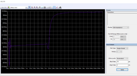
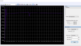
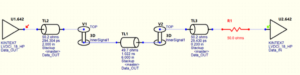
I am running a simulation on a 50 ohm transmission line in free form schematic in which I have a driver and receiver and a transmission line in between. There are also two via on the transmission line. I am running s-parameter analysis. I have attached two graphs at TDR impedance measured at driver node and TDR impedance measurement at the receiver node. What these graphs shows us ? The impedance is not 50 ohm. Is that due to the termination ?
 

Attachments

  • Untitled 395.png
    Untitled 395.png
    32.6 KB · Views: 44
  • Untitled 396.png
    Untitled 396.png
    31 KB · Views: 44
I am simulating to see TDR impedance response. I have probed at both driver and also at receiver but it look like this impedance is not same over time. It should be constant over time in TDR response, right ?
 

Attachments

  • Untitled 397.png
    Untitled 397.png
    30.3 KB · Views: 34
If you thought it was the termination R.

Why not confirm that assumption and test it with a passive R = 50 , 75 , or 100?

Then check your setup and calibration and go beyond 2ns.

Via properties to be 50 ohm are typically, height/hole = 2:1, Ref. Plane opening D/ Pad D = 2:1 for FR4
 
@D.A.(Tony)Stewart Thank you very much for your reply. I will try different passive terminations at the resistor between p and n of differential signals. I will also run simulation and see beyond 2ns.

I am not getting the via structure you mentioned. For a 50 ohm FR4 PCB layout you said the ratio between height and hole is 2:1. Is that the height of the dielectric ? I am also not getting reference plan opening. Can you please explain that again ? Thanks in advance.
 
I'm partly confused. You have been initially asking about 20 ohm impedance difference in TDR, obviosly casused by a wrong termination. Now you are looking for impedance discontinuity involved with vias. That's surely an interesting topic, but did you already solve the original problem? You still didn't show a schematic of the overall setup.

The picture in post #5 brings up questions. According to text, it's a via connection to "inner signal". How does the via look exactly? Is it blind via ending at inner signal layer? Or is it back-drilled? Or is it regular through via, not sketched correctly?
 
This is not how one designs a controlled impedance transmission line in your schematic.

1698079839849.png


1. The via must physical properties of height and pad D that affects nH/mm and have a gap to the ground planes on each layer to create an effective stray 3D pF/mm of the gaps a in order to make the Zo² = L/C = 50²

2. The Rx has a programmed shunt R of 50 ohms. It is not shown as series R1.

3. What is the dielectric constant? What are all the physical lengths and widths?

1698080373546.png


4. Assuming Tpd = 58 ps/cm in your dielectric (Er = TBD) a delay of 2.2 ns corresponds to a length of 38 cm where you show a termination of 72 ohms.
5. The low impedance of 37.5 Ohms at 0.1ns or 100 ps implies a excessive capacitance near 17.2 mm from the source.

None of these problems can be resolved without more details on the design assumptions.

Your 2nd plot, I also changed the colour to yellow to see are not labelled as s11 or s232 but show more problems at the source, but more importantly, the wrong impedance.
1698080895073.png
 
Last edited:
I didn't fold out post #8 schematic. Now it's a bit clearer. DCI I/O-standard involves internal source side termination around 50 ohm and usually unterminated load. Optionally external load termination to Vcc/2 can be applied. TDR step to 72.5 ohm doesn't seem right for unterminated load, may be a scaling error. Perhaps the setup can be further clarified. Apparently it's simulated TDR in ADS, I don't exactly understand how it works in combination with DCI driver.
--- Updated ---

Source side termination gives sufficient signal quality for most medium speed digital signals, also discontinuity at vias is usually no problem.
 
Last edited:
Thanks for your comments. The design goal of the terminations at driver and receiver is basically to get constant impedance 50 ohm at the source and destination, right ? Ideally we want a constant impedance probing at the driver and also at the receiver, right ?
 

LaTeX Commands Quick-Menu:

Part and Inventory Search

Welcome to EDABoard.com

Sponsor

Back
Top