Continue to Site

Welcome to EDAboard.com

Welcome to our site! EDAboard.com is an international Electronics Discussion Forum focused on EDA software, circuits, schematics, books, theory, papers, asic, pld, 8051, DSP, Network, RF, Analog Design, PCB, Service Manuals... and a whole lot more! To participate you need to register. Registration is free. Click here to register now.

Switching Regulator Ground Moating

Status
Not open for further replies.

rocky79

Member level 5
Joined
Sep 20, 2010
Messages
83
Helped
1
Reputation
2
Reaction score
0
Trophy points
1,286
Activity points
1,903
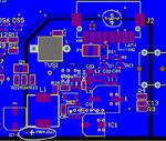
I have a DC-DC switching regulator that operates at switching frequency of 260Khz. It steps down a 28vdc to 3.3Vdc.
On the same PCB I have a microcontroller and would like to have it's ground plane to be as clean as it can be from any switching regulator noise .

Will a ground moat around the switching regulator helps in this case? I will have a 50mil trace that connects the switching regulator ground to the microcontroller ground. Your feedback is appreciated.
Thanks!
Switching_GND Bottom.JPG
 

A separated power ground and ground plane can help to keep commutating currents inside the power supply region. But it's adavantage can be easily dwarted or turned into drawback if you reinject the switching noise along with the input and output power lines between both regions.

We have to look at filter inductors and placement of bypass capacitors to decide about this point.

A digital microcontroller isn't particularly sensitive to switching noise. The need for separate power grounds is usually brought up by high speed or low-level analog circuits of a mixed design. And of course, EMI regulation may enforce the isolation of switcher circuits.

From overall active and passive EMI considerations, a continuous ground plane is preferable. I usually have power ground as additional power plane region (e.g. cut-out of VCC or other power planes) in a multi layer PCB.

I see, thank you for your suggestion.
Here is my switching regulator schematics:
Schematics-Switching-Regulator.JPG
I saw this article (link below) about ground moating topic. Design guide#2 mentions that it's rare where you need to moat which is similar to what you were saying.
https://learnemc.com/tutorials/guidelines/Important_Guidelines.html
 

    V

    Points: 2
    Helpful Answer Positive Rating
Here is my switching regulator schematics.
The separated ground area should be represented in the schematic, preferable by separate PGND net and a net connector, or at least by connected lines and explaining text.
 

You keep the switching loop ground area on the same layer as the components and only connect it to the main ground at one point. Same with the switched main signal. Keep these loop areas (input loop output loop) as small as physically possible and on the same layer as the components then the noise is isolated within the loop to an extent..
That tiny little ground connection will be a high impedance point.
There is a wealth of information and layout notes available from Ti and Linear (to name two) on SMPS layout...
 

    V

    Points: 2
    Helpful Answer Positive Rating
I usually used to route the traces of power supply ground and not connect them to the GND plane. The GND connection at the output filter capacitor of the SMPS will then be connected to the GND plane.

This way i used make sure that there will not be a longer ground loop for the operation of the SMPS and also would be restricting the switching noise getting mixed with the digital circuit GND. For this I had to place the SMPS and its inputs close to the power input connector.
 

Again go and read all the data provided by the controller ICs most specify you join to the main plane underneath the device at the centre of the switching ground formed by the input and output loops.....
 

Status
Not open for further replies.

Part and Inventory Search

Welcome to EDABoard.com

Sponsor

Back
Top