Continue to Site

Welcome to EDAboard.com

Welcome to our site! EDAboard.com is an international Electronics Discussion Forum focused on EDA software, circuits, schematics, books, theory, papers, asic, pld, 8051, DSP, Network, RF, Analog Design, PCB, Service Manuals... and a whole lot more! To participate you need to register. Registration is free. Click here to register now.

[SOLVED] Switched capacitor circuit

Status
Not open for further replies.

electronics_rama

Member level 3
Member level 3
Joined
Aug 8, 2015
Messages
57
Helped
2
Reputation
4
Reaction score
5
Trophy points
1,288
Activity points
1,887
Hi All,

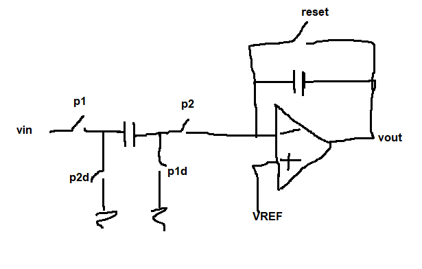
I am simulating the below-switched cap integrator circuit configuration. I have used the verilog-A model for the amplifier. Whenever I set VREF as 0V, I see the vout integrating the output properly. If I set the VREF anything other than 0V, I see VOUT as not an integrated value of the input. What is that I am missing here? Can anybody help?

1651058443293.png


Thanks,
Rama
 

In the first estimation, vout = -integ(vin-vref)

Any particular equation with which you arrived at this conclusion?
Because, I am seeing the result as,
vout = integ(vin+vref)

I have kept the cap values as same. Input is kept as 100mV DC. Vref has been kept as 500mV. I see the integrating step close to 600mV.
 

I applied the charge balance equation and arrived at the following conclusions,
1651129769171.png


When p1=1 & p2 =0,
Q1=vin*C1, Q2 =0
When p2 =1 & p1 =0,
Q1’ = (0-vn)*C1 = -vref*C1, as vn = vref because of virtual ground.
Q2’ = (vout-vn)*C2 = (vout-vref)*C2

Applying charge balancing,
Q1+Q2 = Q1’+Q2’
Vin*C1 = -vref*C1 + (vout-vref)*C2
vout*C2 = vin*C1 + vref*C1 + vref*C2
vout = (C1/C2)*vin + (1+C1/C2)*vref
Before the start of the integration, vout_intial = vref.
Thus the integrating step is,
vout – vout_initial = (C1/C2) * vin + (C1/C2) * vref
Integrating step = (C1/C2) * (vin + vref)


Now, when vp = vref,
1651129844612.png


When p1=1 & p2 =0,

Q1=vin*C1, Q2 =0

When p2 =1 & p1 =0,

Q1’ = (0-vn)*C1 = -vref*C1, as vn = vref because of virtual ground.

Q2’ = (vout-vn)*C2 = (vout-vref)*C2
Applying charge balancing,

Q1+Q2 = Q1’+Q2’

Vin*C1 = -vref*C1 + (vout-vref)*C2

vout*C2 = vin*C1 + vref*C1 + vref*C2

vout = (C1/C2)*vin + (1+C1/C2)*vref

Before the start of the integration, vout_intial = vref.

Thus the integrating step is,

vout – vout_initial = (C1/C2) * vin + (C1/C2) * vref

Integrating step = (C1/C2) * (vin + vref)


With the vref as the opamp input reference, indeed the integrating step will be (C1/C2)*(vin+vref). From the equations it becomes clear. But still are there any intuitive explanations why the vref is coming in the integrating factor?
 

I would recommend to tie both the front end grounds to vref (suggested earlier), and bias the vin at vref.
Then

Q1: (Vin+Vref-Vref)C1
Q2: (Vref-Vref)C1-(Vref-Vout)C2
Q1=Q2
VinC1 = -VrefC2 + VoutC2
Vout = Vin(C1/C2)+Vref

This way your output will only have a constant offset of Vref with integrating term Vin(C1/C2) on top of it (like biasing a single rail opamp output at the center, which is why you'd need input vref anyways).

If you do it the way you show earlier, you have the Vref term also integrating, causing your opamp to saturate to a rail quickly. The vref comes into the integrating factor in your version, because you never provide a means to subtract it out.
 
Last edited:
Yes, I changed the grounds to vref and I added the vref to the input. Now, I can see the integrating step as (C1/C2)*vin with the initial voltage offset as vref.

Thank you all for helping me to have a solid understanding of this.

Thanks,
Rama
 

Status
Not open for further replies.

Part and Inventory Search

Welcome to EDABoard.com

Sponsor

Back
Top