Continue to Site

Welcome to EDAboard.com

Welcome to our site! EDAboard.com is an international Electronics Discussion Forum focused on EDA software, circuits, schematics, books, theory, papers, asic, pld, 8051, DSP, Network, RF, Analog Design, PCB, Service Manuals... and a whole lot more! To participate you need to register. Registration is free. Click here to register now.

Switch a LED using a NPN Transistor

Status
Not open for further replies.

giovaniluigi

Member level 1
Member level 1
Joined
May 30, 2009
Messages
32
Helped
0
Reputation
0
Reaction score
0
Trophy points
1,286
Visit site
Activity points
1,626
This seems to be a very basic question, but I'm having certain doubts.
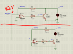
NPN_LED.PNG

From the picture above you can see 2 configurations to turn on/off a LED.

I would like to know what is the correct/best design, or what is the difference between them, in except of the inversion of the signal...

I'm not sure how I should use, or if both are ok.

I'll use this to drive a LED from an optocoupler at 20Khz.
Which one should I choose for best performance ?
 

I suggest you to go with Fig:2 because of the open collector configuration. The first circuit will be preferred for logical output. The first circuit will also works, but unnecessary power dissipation will happen across the resistor even if the LED turn off...
 

hmm, yeah I see, there is a current flowing always on the circuit 1.
But, why do you think that it is a better choice for logical output ?
Also, in the case of a digital output, should I be concerned with the voltage drop on the BJT transistor ?
 

You are driving the transistor base with about 1/10 of the collector current for a forced beta of 10 (the typical recommended value) which will give good turn-on of the transistor well into saturation. For that, the output Vce drop of the transistor when ON should be less than a tenth of a volt.
 

You are driving the transistor base with about 1/10 of the collector current for a forced beta of 10 (the typical recommended value) which will give good turn-on of the transistor well into saturation. For that, the output Vce drop of the transistor when ON should be less than a tenth of a volt.


Ok, I see, so the drop is basically dependent of the BETA.
Do you have a pratical way to calculate this drop ?

I mean, if I put 12V on the collector, with 1mA as I(be) what should be the drop expected on the transistor ?

Thanks.
 

The beta used to insure saturation is a forced beta (beta lower than the data sheet values). A typical value used for this is 10.

You can determine the drop by estimating from the data sheet saturation voltage values or use a Spice simulator such as LTspice.


Edit: If you put 12V on the collector with no load, then the transistor will never saturate, by definition.


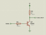
Yeah I see, but someone told me, that for example If I put a BJT in this configuration here:

NPN_LOGIC.PNG

A person told me that when this NPN is conducting in the circuit above, I'll always have an offset of 0.6V on the "TO MCU INPUT" probe, which means that I'll never have 0V on it.
So if I connect a digital pin like an input of MCU on the "TO MCU INPUT" it will never go down to 0V it will always be 0.6V from GND due to the BJT drop. Is that true ?
So my digital port will work between 5V for ON and 0.6V for OFF state.
I personally don't agree. What do you say about that ?
 

Not true. That "person" is a poor source of electronic information so please avoid him/her for such questions. The Vce ON voltage of the transistor should be less the 0.1V for that circuit. Perhaps the confusion is that Vce can be less than the Vbe ON voltage which is 0.6 to 0.7V typically.
 

Thanks.

Well there is only one more question, the heat produced by the BJT is due to the small drop of voltage causing a resistence to the current I(c) right ?
Also, to avoid the waste of energy in heat dissipation, I should ensure proper saturation, correct ?
 

Yes. With proper saturation of the transistor the waste heat will be very small. For example 5mA with a 0.1V drop is only 0.5mW. That raises the temperature about 0.1°C for a typical small transistor case which is too low to feel.
 

Status
Not open for further replies.

Similar threads

Part and Inventory Search

Welcome to EDABoard.com

Sponsor

Back
Top