Continue to Site

Welcome to EDAboard.com

Welcome to our site! EDAboard.com is an international Electronics Discussion Forum focused on EDA software, circuits, schematics, books, theory, papers, asic, pld, 8051, DSP, Network, RF, Analog Design, PCB, Service Manuals... and a whole lot more! To participate you need to register. Registration is free. Click here to register now.

Surface Finish on Microwave PCBs

Status
Not open for further replies.

youngguns21

Member level 2
Joined
Jun 7, 2010
Messages
42
Helped
0
Reputation
0
Reaction score
0
Trophy points
1,286
Activity points
1,630
I'm a designer having a discussion with a coworker who's background is PCB manufacturing.
On our PCB fab drawings we call out IPC-6018 with an ENIG finish and I questioned him on why we aren't using electrodeposited Ni/Gold.

He replied that we only use SMT chips (no wire-bonding) and the thicker gold would cause Gold Embrittlement. He also stated that the under-cut from the etch on electrolytic Ni/Gold is not as well controlled which will cause the filters I pattern to have a larger tolerance than what I design them for.

Should I be pressing harder for Ni/Au over ENIG? My current board is operating around 5.5G.

If you're a microwave guy/lady, please chime in. Thanks
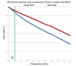

@ 5.5 GHz, the surface finish will have negligible impact wrt Insertion Loss. Nickel in general, is the unwanted metal. As it behaves ferromagnetically at saturation frequencies.
 
Last edited:

ENIG.png

I should add. The Y scale is dB/inch. So, approximately ~0.15 dB per inch delta vs bare Cu . Which can be significant depending on total TL length. Albeit, if there are higher order harmonics of interest, ENIG can have substantial impact to IL. It really depends on trace width, and total TL length.
 
Last edited:

I have seen few 'yellowish"-plated RF pcbs which was manufactured 5 to 10 years ago. Maybe it was gold plating or one of those you mentioned. All boards had an unpleasant corroded look, like someone spilled water on them, dried up and left dirt stains. I wonder how it happened, equipment was from two different respectable manufacturers, in hermetically sealed plastic enclosures and additional machined internal shields (not hermetic though). Most of corroded look was near screw mounting holes. Maybe some chemicals was not washed properly during the process.

After that i have doubts about using gold plating option provided by different PCB fabs. Who knows how you PCB will look after few years if not properly immersed. Interestingly to note: one PCB fab insisted on using gold plating for Rogers material. Explaination was that their tin plating process may cause some kind of PCB warping and even traces peel off on Rogers RO3004/4350.
 
Last edited:

ENIG has a thick nickel and VERY thin gold layer. That will be very lossy at microwave frequencies. So if you have circuits that need low loss (or high Q), ENIG will not work well.

IF you put a thicker layer of gold on top, then more of the top surface currents will be in the thicker gold layer, and the loss will be much less. And yes, solder typically WILL leach the gold and cause embrittlement.

I have never used it, but apparently immersion silver is best for both corrosion and microwave loss:

https://www.microwavejournal.com/bl...nish-makes-a-difference-in-broadband-pcb-loss

https://www.microwavejournal.com/bl...8-off-to-the-races--creating-winning-finishes
 
Last edited:

ENIG has a thick nickel and VERY thin gold layer. That will be very lossy at microwave frequencies. So if you have circuits that need low loss (or high Q), ENIG will not work well.

IF you put a thicker layer of gold on top, then more of the top surface currents will be in the thicker gold layer, and the loss will be much less. And yes, solder typically WILL leach the gold and cause embrittlement.

Yes and no. Around 20 GHz+ The skin depth is so shallow, the bulk of the current is in the gold, not the nickel. And the IL curve begins to match the bare Cu losses. From ~3GHz+ ENIG begins to drop away from bare Cu on an IL plot, the "knee" frequency, where the substantial drop occurs is around ~5 GHz and drops off thereafter with a relatively steep gradient. Trace width and dielectric material contribute to the magnitude of loss. ENIG degrades IL, but @ 5.5 gHz it's roughly 0.1-0.2 dB per/inch for typical trace width and laminate material. It all depends on what your loss budget will allow.
 

ENIG has a thick nickel and VERY thin gold layer. That will be very lossy at microwave frequencies. So if you have circuits that need low loss (or high Q), ENIG will not work well.

IF you put a thicker layer of gold on top, then more of the top surface currents will be in the thicker gold layer, and the loss will be much less. And yes, solder typically WILL leach the gold and cause embrittlement.

I have never used it, but apparently immersion silver is best for both corrosion and microwave loss:

https://www.microwavejournal.com/bl...nish-makes-a-difference-in-broadband-pcb-loss

https://www.microwavejournal.com/bl...8-off-to-the-races--creating-winning-finishes

Thanks, Biff44.
So are there options to mitigate the embrittlement?
Also, I've done a few things with immersion silver where I was fighting for every 0.1dB. Silver tarnishes quickly, have to use solder or silver wirebonds, and I litterally only got a few tenths of a dB out if it. Perhaps if the entire board was silver I would have done better, but we were not set up for silver wirebonding.

- - - Updated - - -

Yes and no. Around 20 GHz+ The skin depth is so shallow, the bulk of the current is in the gold, not the nickel. And the IL curve begins to match the bare Cu losses. From ~3GHz+ ENIG begins to drop away from bare Cu on an IL plot, the "knee" frequency, where the substantial drop occurs is around ~5 GHz and drops off thereafter with a relatively steep gradient. Trace width and dielectric material contribute to the magnitude of loss. ENIG degrades IL, but @ 5.5 gHz it's roughly 0.1-0.2 dB per/inch for typical trace width and laminate material. It all depends on what your loss budget will allow.

Thanks, Airbag79. Thats some really good info. Any chance you have a reference for that?
 

Thanks, Biff44.
So are there options to mitigate the embrittlement?
Also, I've done a few things with immersion silver where I was fighting for every 0.1dB. Silver tarnishes quickly, have to use solder or silver wirebonds, and I litterally only got a few tenths of a dB out if it. Perhaps if the entire board was silver I would have done better, but we were not set up for silver wirebonding.

- - - Updated - - -


Thanks, Airbag79. Thats some really good info. Any chance you have a reference for that?

Unfortunately, no. This is all empirical data, from my own design experience. It is proprietary.
 

yep silver does oxidize. If it was a "cost is no object' military application, I guess you could do a rhodium flash over the silver. That would keep the silver from tarnishing. All the old Baytron millimeter wave waveguide pieces were finished that way.
 

.......................IF you put a thicker layer of gold on top, then more of the top surface currents will be in the thicker gold layer, and the loss will be much less. And yes, solder typically WILL leach the gold and cause embrittlement.......................


presumably that was referring to normal Pb/Sn solder ?
if so would silver soldering overcome the embrittlement problem ?

just curious

Dave
 

presumably that was referring to normal Pb/Sn solder ?
if so would silver soldering overcome the embrittlement problem ?

just curious

Dave

Yes, that's using Pb/Sn. Im not sure about Ag solder. I would imagine the gold would still leach to an extent, but you would have to look into the effect Ag/Au have on each other (aka dissimilar metals interaction)
 

many metals will dissolve into gold, and vice versa. Tin is a big one that READILY combines with gold.
Watching gold leach into Tin/Lead eutectic solder is just like watching sugar dissolve into coffee!

The problem is if you have a eutectic solder....maybe some sort of tin-lead free combination, IF gold dissolves into it, it screws up the metal at a molecular level. You no longer have the eutectic chemical composition you wanted, so the reflow temperature goes way up--often resulting in a cold/non-wetted solder joint. And since you now have a mix of gold/solder mix, and regular solder, in the joint, those grain boundaries can fracture at the slightest mechanical stress.

In other words...you do not want it. So you limit just how thick the gold layer is plated on top of the nickel.

IF you HAVE TO use thick gold, there are some solder alloys that do not leach the gold very much--primarily indium alloy solders
 

Why don't you just use selective plating? Have gold plated where you want/need it, ENTEK where you don't. I used to get boards with gold plated test points and connector pads - the rest was ENTEK.
 

Another approach would be making design that will withstand bigger tolerances in manufacturing process. I think at 5GHz replacing some parts for more gain can cost less than using gold plating. And it is good to have PCB design than can be manufactured almost everywhere.
 

Status
Not open for further replies.

Part and Inventory Search

Welcome to EDABoard.com

Sponsor

Back
Top