Continue to Site

Welcome to EDAboard.com

Welcome to our site! EDAboard.com is an international Electronics Discussion Forum focused on EDA software, circuits, schematics, books, theory, papers, asic, pld, 8051, DSP, Network, RF, Analog Design, PCB, Service Manuals... and a whole lot more! To participate you need to register. Registration is free. Click here to register now.

Strange problem with Cadence!

Status
Not open for further replies.

chandra3789

Member level 1
Joined
Jun 11, 2011
Messages
36
Helped
0
Reputation
0
Reaction score
0
Trophy points
1,286
Location
kharagpur
Activity points
1,622
hi ....i need your help.....
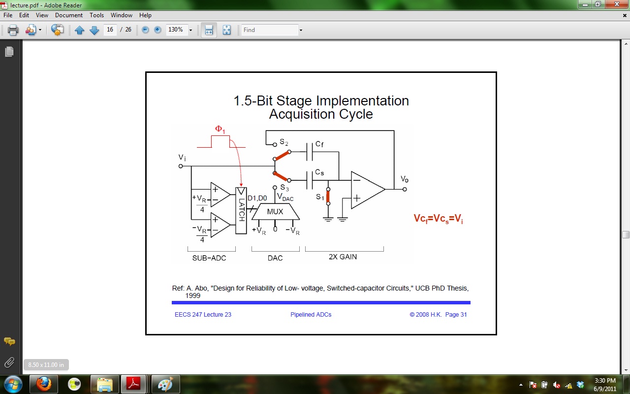
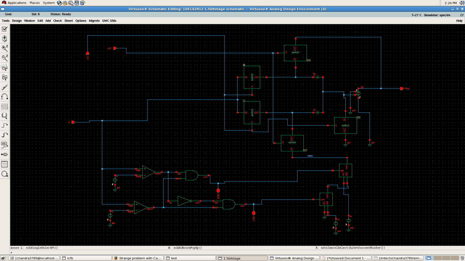
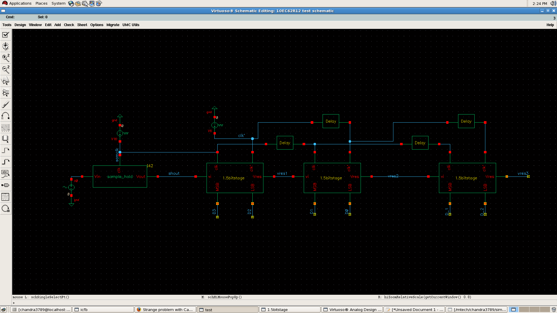
i am trying to simulate 12 bit pipelined ADC using ideal blocks from AHDL library in cadence libraries.....
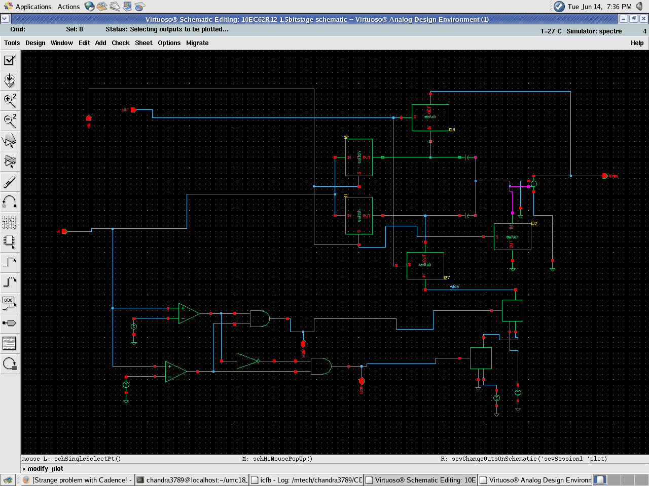
i am using 1.5bit/stage topology with 10 1.5 bit/stages and 2 bit flash at the end...
while simulating it i am getting a weird problem.i first simulated single stage with DC, ramp and sinusoidal inputs, it worked fine. when i added one more stage and simulated those two stages it worked fine and the simulation completed in a very less time.
but when i add one more stage i.e., 3 stages , the transient simulation is taking very very large time(almost infinite) and its never ending.
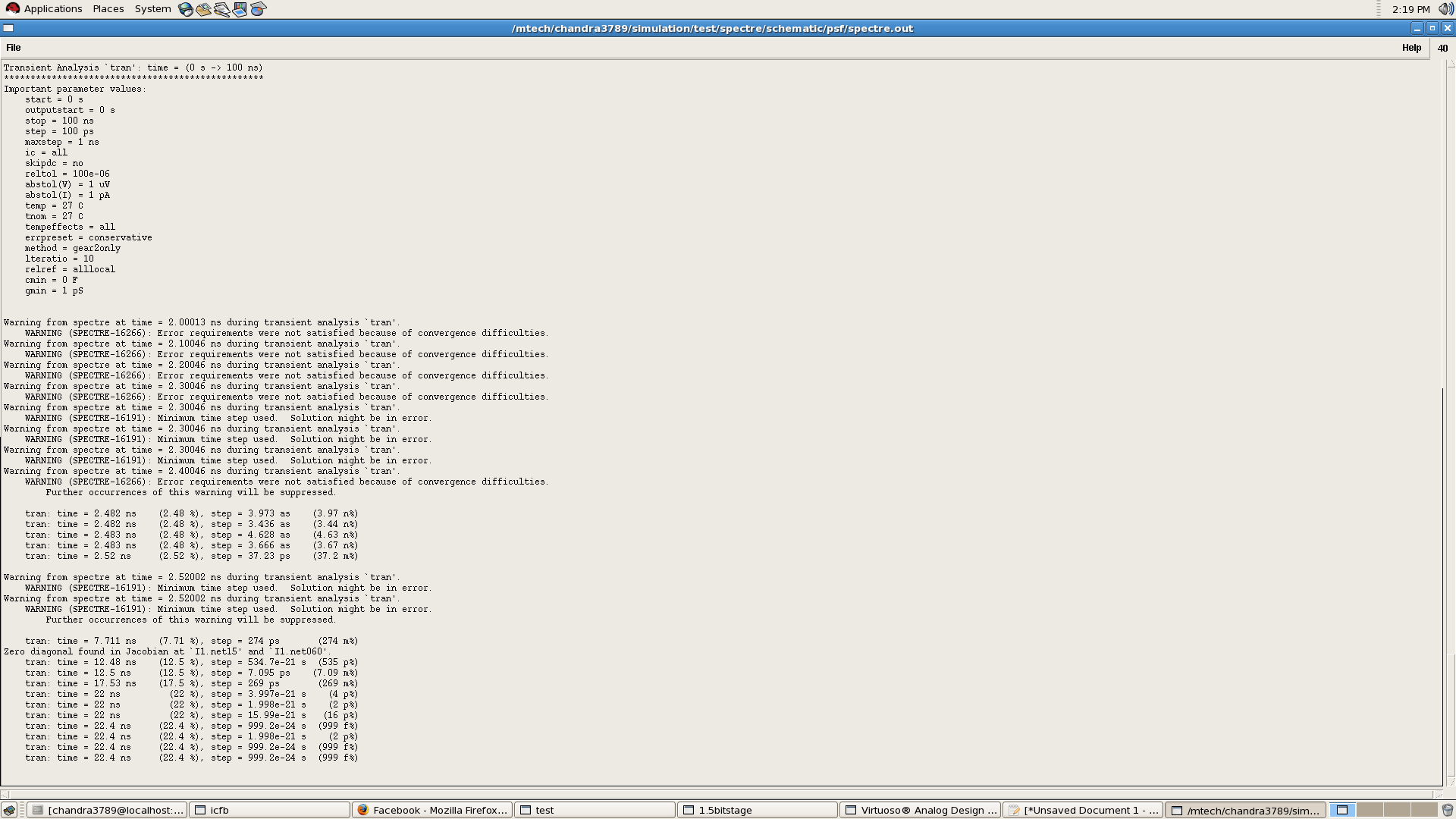
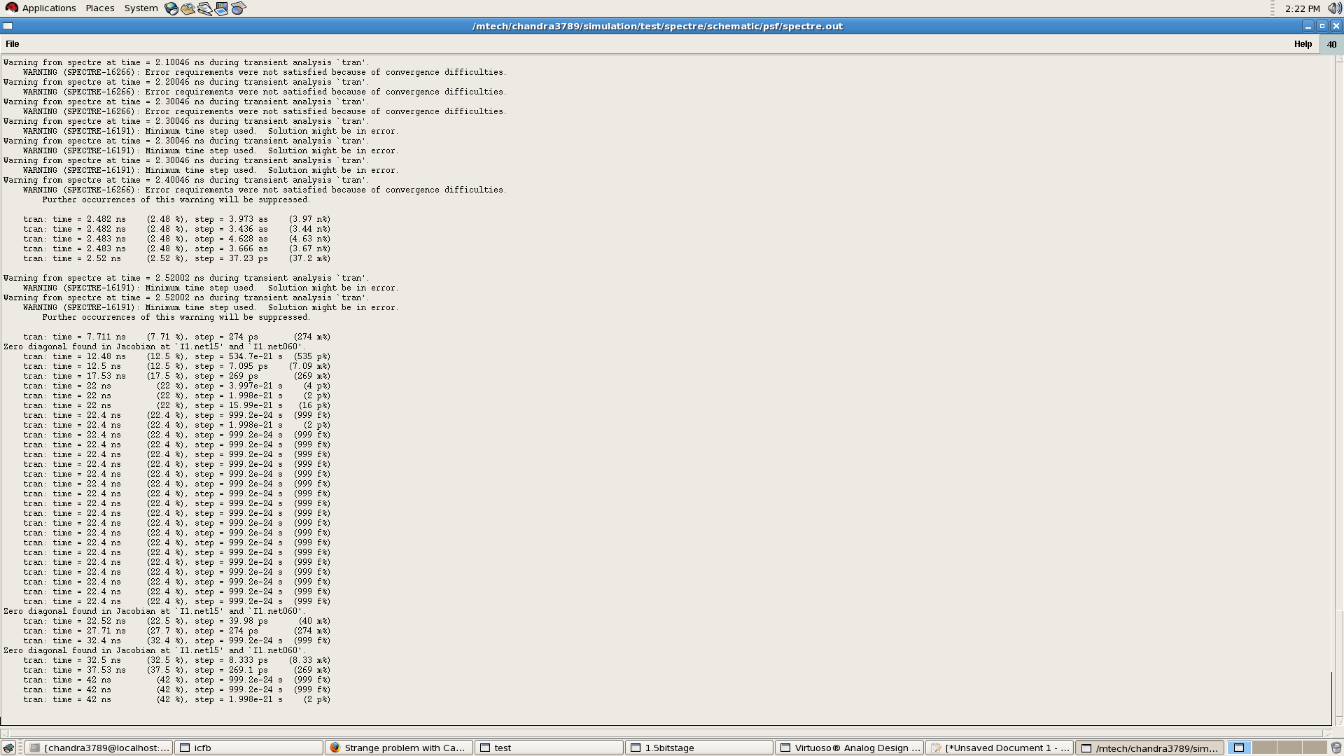
if i give 100ns it generally takes 2ns step but at 2.001 ns the step size is falling down to 8.2e-21 s!.....
if i give 20ns it is simulating fine upto 12ns and the step size is falling down to 8e-21 s!....
no errors and warnings are being shown during the simulation.........
this is a weird problem which i have never seen........
have you any idea why?........
more over why its happening when i do it for 3 stages only? why not for 2 stages?
replies are most awaited.
 

what accuracy settings are you using?

If accuracy is not the issue, consider that the problem is showing up only when you have a stage sandwiched in between two stages which might indicate that
- the ideal load used on the final stage is too different from the actual load experienced when stage-loaded
- the ideal spice source impedance is too different from the actual impedance provided by a stage to the next
- the kick back from a stage is triggering instability

The final point is probably triggered by the previous two

You are probably using a x2 amplifier to generate the residue for the following stage, is this continuous time?
 
sir yes i am using a *2 amplifier which is switched capacitor based and it not continuous one.its track and hold phases are non overlapping. The residue is generated only in the hold phase.also i am using T/H circuit before the first stage. The 1.5 bit stage i am using is shown below.

the load i am using at the end of last stage is zero i.e., i just kept the output of the 3rd stage floating and ran the simulation.If the problem is because of the then why didn't that problem show up when i used 2 stages?..
thanks for your precious time.......

---------- Post added at 14:29 ---------- Previous post was at 14:17 ----------

Also strangely it is showing errors = 0 and warnings = 0 before simulation starts.
 

Hallo chandu,

well the switched cap makes it somewhat more interesting to verify stability, right?

What settings are you using for the ideal OTA? do you set an output resistance or poles?

In any case try to push the voltage/current/charge/timing accuracy to get to the end of your simulation or at least further along so you can see if anything oscillates
 
There is no feedback from output to the input, since the output is zero during the track phase and input is left floated during the hold phase. So literally they are not connected as they are driven by two phase non overlapping clocks. well, i think the problem is due to convergence but if the problem is due to that the simulator would surely show that "the solution might be in error""error requirements are not satisfied" kind of errors but errors are shown to be zero. One of my friends suggested me to change mode of transient analysis from 'conservative' to 'liberal'. Do you think this will help?
i am using an ideal VCVS from analog lib in place of op amp.......i checked it thoroughly, it works fine......i didnt give any settings except maximum and minimum output voltages..
 

I thought you were using ahdl models, if you know the x2 amp is stable by design during the phase where the simulator stops then the issue might come from the latch, how is this modeled? is there any hysteresis in it?

The OP was found because TRAN started, you seem to have a problem with transient step and analog accuracy, if anything I would increase the accuracy of the simulation not reduce it

Since you are using switched caps make sure you are using a charge conservation model, I am not too familiar with spectre so you'll have to do some digging in the manual for that

what gets switched on when your TRAN stops? what phase are you in?
 
with ideal components the latch is not required provided that the delay of the comparators is less than the track time of the clock. SO i made sure that and removed the latch and it worked well.
The simulation is stopping in track phase only.....!!!

---------- Post added at 10:56 ---------- Previous post was at 10:46 ----------

when i simulated it by changing the tran analysis mode to liberal then it showed the error
"no convergence achieved with the minimum step specified. Last acceptable solution computed at 21.004ns"........!

---------- Post added at 11:26 ---------- Previous post was at 10:56 ----------

also is shown "zero diagonal found inside the jacobian at net 12 and net 15".....what does that mean?
 

boy spectre really does ****, is it the only simulator you have available? how about hspice? or even better eldo?

in any case you are still not mentioning your accuracy settings, I guess you are using defaults, which would be bad since default accuracy is 0.1% in spectre

as of the latch, sorry I misread your diagram I thought latch indicated a latched comparator, how are you modeling the comparators?

The errors you are getting are from lack of convergence during tran, the nets implicated might be a good indication of where the problem lies

I am reading the presentation you are using as a reference, I will see if that gives me a better guess of where your problem might be
 

sir this is the error i am getting....


---------- Post added at 12:22 ---------- Previous post was at 12:19 ----------

i did not give any accuracy settings.........the main question is if all those things matter why didnt the error showed up for two stages....
in the errors it is shown zero diagonal.....like this......
........

---------- Post added at 12:24 ---------- Previous post was at 12:22 ----------

the schematics i am using for 1.5 bit/stage and test are........
 

what are those delays at the top? shouldn't clk become clk' of the following stage and viceversa? I understand that when one stage is in acquisition the following one is in conversion and viceversa, correct?

reltol is now at 100e-6, I would probably push it to 1e-6 to be safe

also a minimum output resistance on the opamp might help with infinite bandwidth problems

my best guess is that the stage in the middle is experiencing some sort of instability at a frequency so high spectre cannot resolve it at the minimum time step

which nets are I1/net15 and I1/net060?
 
Actually because of the ideal blocks i got some synchronization error and the outputs of the second and subsequent blocks were becoming zero because of very little delay of the ideal blocks......so for synchronization aid i intentionally inserted some delay and it resolved that problem.......
i understand it like this....
during track phase of the clock all the residues are zero(ideally if there ain't any offset) because of the switch that connects the opamp (-)terminal to ground.....
during the hold phase the residues are evaluated as a function of the input to that stage and will be passed on to the next stage.......
plz correct me if what i understood is wrong!

---------- Post added at 13:50 ---------- Previous post was at 13:43 ----------

The problem is with net 12, net 15 and net 78 in the 1.5bit stage schematic.......
net 12 and net 15 are the wires which connect the left plate of the capacitors to the switches and net 78 is the wire which connects their right plates......
 

yes sir you are right....for reducing the latency by half we can drive consecutive stages by alternate clocks.....sorry i did not check that while reading the literature.....
ok then i would change it and see if the same error comes again.....
 

i did simulate with two stages with alternate clocks.but this time the error has shown up with 2 stages itself........
It is showing convergence difficulties again.......damn
convergence failure in net 15 and net 60.........those nets are....

......
the nets that are shown in green and red kin colors connecting to the capacitors.........
 

what is the gain of you ideal amplifier (vcvs)?
keep it realistic say 1000-10000
can you try also adding a resistor in series to its output say 100kOhm and also add a capacitor (say 1pF) to ground after the resistor?
This will generate a single pole response at f=1/100k/1p/2/pi~1.6MHz
have you pushed reltol to 1e-6?
can you confirm that the stage where these nets failed convergence was entering acquisition mode when this happened?
 
yes they are in track mode when convergence is failing.....and to my surprise the currents in those nets are growing indefinitely ..that is the reason for convergence failure....
and i don't know even a bit about reltol...what is that......sorry i am not that familiar with cadence simulations!
 

the problem might come from infinite voltage slew rate then, in that case adding the output pole as described above should help
 
yeah i would do that and see......but the pole you are saying wil be at 1.6 MHZ ..but i am trying for around 80-100MSPS speed.....so will that effect .......The DC gain i have given is 10000...so roughly UGB will be around 160MHZ.....okay that may work fine.....will check it tomorrrow and post it........i really thank you for your valuable time ......
 

sir i dont know how to thank you........it worked .........that was a great help.......
 

that's very good news chandra hope your design goes well, we have recently submitted a similar design, now we hope silicon will be forgiving...
 

I simulated 10 bit pipelined ADC with 1.5bit/stage architecture with ideal blocks and now want to move on to its transistor level implementation...while simulating it with ideal blocks i got some basic doubts......please clarify them
1) i am using 0.18um cmos9t5v technology....
in 1.5 bit stage architecture as shown below we need two comparators one with positive VRef/4 and the other with -VRef/4 thresholds and

my input signal can range from -vref to +vref which means i can give a double polarity(both +ve and -ve) signal as input...
hence if u want to pass a signal which has two polarities your op amp which u use in S/H circuit should allow to pass them which means that the op amp has to have power supplies -0.9V and +0.9V.....
because if we use 0 and 1.8V supplies the ICMR of the op amp would be positive somewhere symmetric about 900mV and hence it cannot pass negative signals!......
one more doubt which makes my above question strong is since the residue we pass from one stage to the next can be positive or negative the op amp must be able to give negative as its output which means that op amp must have two supplies +0.9V and -0.9V but in almost all the publications i saw they showed op amps driven by 1.8V and gnd!....
so my question is should i use two polarity supplies or single supply for all the blocks i will be designing?.....i am really in confusion please help me......


2) if we use differential implementation should i go for differential op amp design or single ended one?
 

Status
Not open for further replies.

Part and Inventory Search

Welcome to EDABoard.com

Sponsor

Back
Top