Continue to Site

Welcome to EDAboard.com

Welcome to our site! EDAboard.com is an international Electronics Discussion Forum focused on EDA software, circuits, schematics, books, theory, papers, asic, pld, 8051, DSP, Network, RF, Analog Design, PCB, Service Manuals... and a whole lot more! To participate you need to register. Registration is free. Click here to register now.

STM32F7 CRYSTAL OSCILATOR GND and 3.3v Plane isolation

Status
Not open for further replies.

robokishan

Newbie
Joined
Oct 23, 2020
Messages
2
Helped
0
Reputation
0
Reaction score
0
Trophy points
1
Activity points
19
Hello I have developed pcb in kicad for stm32f765. I am using 16Mhz crystal oscilator for the application. But i am having some confusions regarding the gnd and 3.3 plane.
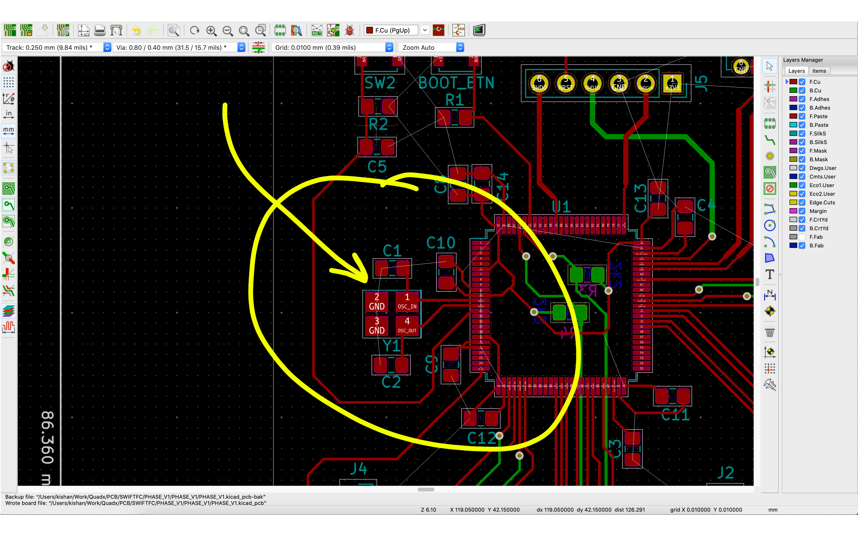
Screenshot 2020-10-23 at 4.01.40 PM.png

As mentioned in the image there is 16Mhz crystal. I want to make 2 layer pcb since budget is tight. and for the first layer which is red if i do ground isolation. can i make second whole plane 3v3 even under the crystal ? or i have to avoid 3v3 plane under the crystal.

Thank you. I don't how do i achieve this.
 

There can't be GND and 3.3V planes on a two layer board. You have already some traces at bottom side. At best you can realize a combination of copper pours on top and bottom implementing a meshed ground. This can probably work for a hobby project or a test board if you don't need to comply with EMI standards.
 

Hi,

I agree with FvM.

GND vs 3V3 under the XTAL. It makes no difference.
* It is isolated thus no DC current can flow.
* GND and 3V3 are AC coupled thus the same AC current will flow.

My recommendation:
Use green layer as GND. Avoid as much as possible other signal - or at least make them as short as possible.

My personal taste: I don´t like copper pour, because it just looks like a solid plane but electrically it isn´t much better than wide traces.


Klaus
 

Thank you Yes. This is the first prototype it doesn't have to comply with any EMI standards as of now. Currently, it is for testing purposes. And stm32f765 will run on 216Mhz so that is why the signaling concerns me.
@FvM thanks for the suggestion
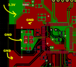
@KlausST Can I use GND as the Bottom layer, 3.3v as the first layer only some portion so that I can avoid any kind of interference. ?

I don't want to comply with any EMI Standards as of now since this is the first prototype testing board. if this works I can go ahead with 4 layer PCB.


Something like this I have attached a screenshot over here
 

Attachments

  • Screenshot 2020-10-23 at 6.01.50 PM.png
    Screenshot 2020-10-23 at 6.01.50 PM.png
    163.1 KB · Views: 83

HI,

I can only repeat what I have written in post#3.
Currently the green layer is far from being a solid GND plane.

Besides this I see no need for a 3V3 plane as long as all supply pins are properly bypassed with suitable capacitors and short connections to GND plane.

Klaus
 

Status
Not open for further replies.

Part and Inventory Search

Welcome to EDABoard.com

Sponsor

Back
Top