Continue to Site

Welcome to EDAboard.com

Welcome to our site! EDAboard.com is an international Electronics Discussion Forum focused on EDA software, circuits, schematics, books, theory, papers, asic, pld, 8051, DSP, Network, RF, Analog Design, PCB, Service Manuals... and a whole lot more! To participate you need to register. Registration is free. Click here to register now.

stitching via

engr_joni_ee

Advanced Member level 3
Joined
Nov 3, 2018
Messages
750
Helped
2
Reputation
4
Reaction score
4
Trophy points
18
Activity points
6,229
I have found some text regarding stitching via. I am wondering how about if the two reference planes are power planes with different voltages on them. Can we also put stitching via using capacitor between them if a high speed signal is routed over the split ? How about if we have 1.8 V and 3.3 V as reference power planes for high speed signal ?

Can this be two ground planes ? for example analog ground plane and digital ground plane ?

In case they are power and ground plane then it's fine to use decoupling capacitors. But how about if both of them are power planes or both of them are ground planes ? Can we use capacitors to stitch them ?
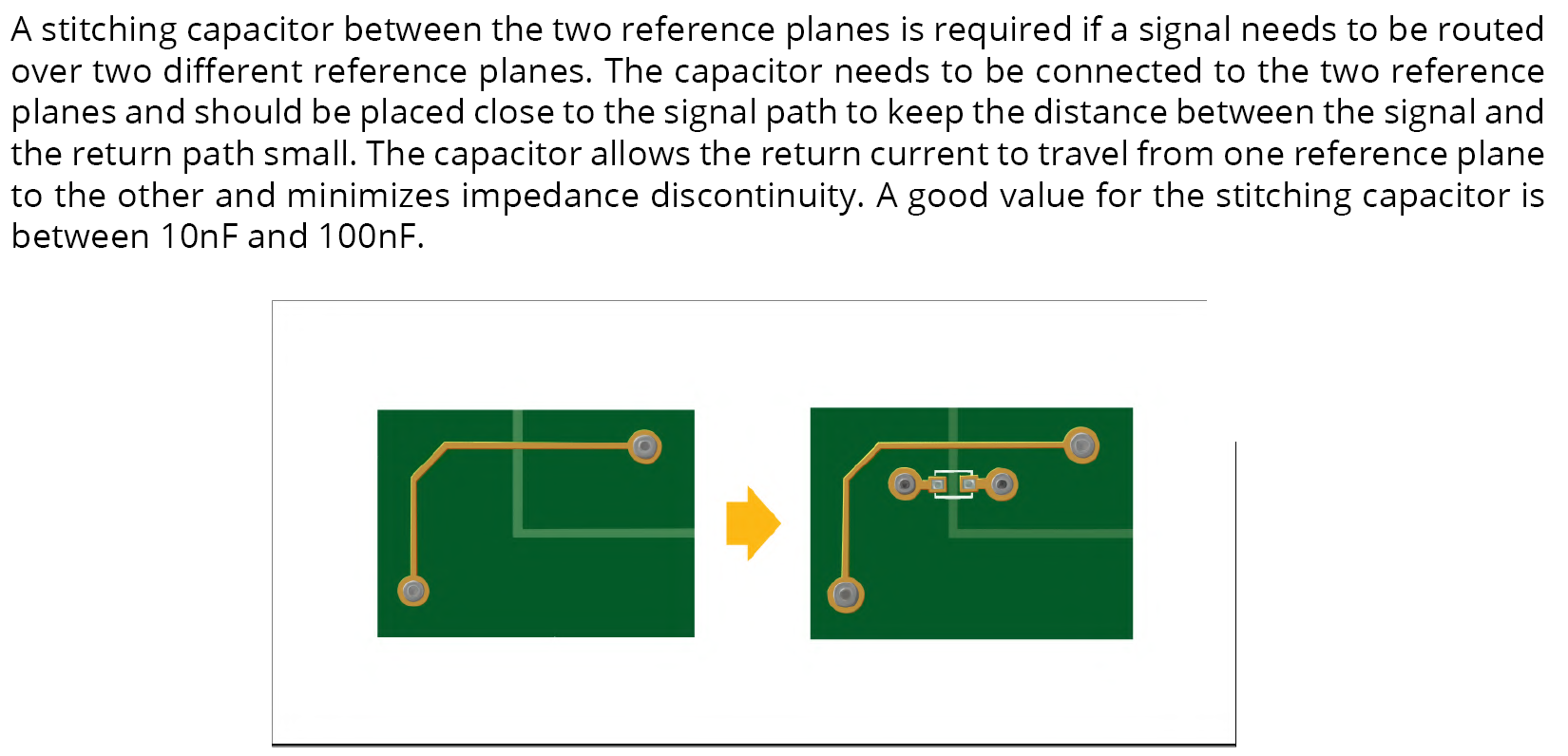
1700815409434.png
 
Hi,

you always have to keep in mind where your return-current is traveling back to its source. For DC and quite low frequencies, the return-current is taking the path with the lowest RESISTSANCE, where for higher frequencies the path of lowest IMPEDANCE will dominate [1]. So here it depends if there is a return path provided in an other layer e.g. GND plane in a layer below. The mentioned stitching capacitor will help if return-current path is required if signals with higher frequencies are involved. E.g. for a signal with a frequency of e.g. 1MHz corresponds to an impedance of 1.59 Ohm @ 100nF. So even if you provide such a sticthing capacitor, the return-current might travel an other way, if available, if it provides a lower impedance. This might disturb for example sensitive analoge electronics.

[1] https://www.protoexpress.com/blog/current-return-path-signal-integrity/

BR
 

    FvM

    Points: 2
    Helpful Answer Positive Rating
Consider two case:

[L1: Signal L2: Ground]: If we route a signal on L1 and these exist a split in Ground plane in L2. Can we mount a capacitor on L1 with both terminals connected to Ground plane through via ?

[L1: Signal L2: Power]: If we route a signal on L1 and these exist two power planes in L2 at different voltage levels. Can we mount a capacitor on L1 with both terminals connected to voltage levels each power plane through via ?
 
Hi,
[L1: Signal L2: Ground]: If we route a signal on L1 and these exist a split in Ground plane in L2. Can we mount a capacitor on L1 with both terminals connected to Ground plane through via ?
this doesn' make sense. If both terminals of the capacitor are connected to GND, the capacitor has no use at all (it is shorted).


A sketch might help to clarify your scenarios.
 
But then what are these two planes which are shown in the original post having a capacitor between them ?

I assume these planes are located on inner layer while the signal trace is located on the top layer.
 
This we only can assume. The two planes might be located on the top layer and covered with solder-resist. As we do not know how this VIAs are connected, we can not give feedback on the actual connection of the planes and the return path.

Where is this screenshot taken from?
 
The picture is a simplified example, sketched to illustrate a problem and a possible solution method. It's not discussing design details and you should not read them into it.

It's just a signal trace with splitted reference plane. At this level of abstraction, it's irrelevant if the planes are assigned to ground or supply potential, just something static.

A real design has multiple planes with multiple connections and "stitching" capacitors.
 
I do understand that the real design have multiple planes. But having stitching capacitor via this I have not seen to be honest and that is the purpose of posting this question to please explain in which cases we can use the stitching capacitor via ? Thanks in advance.
 
Hi,

I´m with marce´s reply .. as general answer about the capacitor´s function.
The other replies point into the same direction.

If you want to talk about details, then please answer stenzer´s question: "Where is this screenshot taken from?"
Then we all have the same context for a discussion.

Otherwise we have to guess .. but I don´t like guessing in electronics design.
Good, detailed answers require good informations first.

Klaus
 
I have attached "General High Speed Signal Routing" a TI document revised Feb 2023.

Section 2.4 describe that there should be no void and no slit in the reference planes. The pictures are shown in Figure 2-6 and Figure 2-7 respectively.

And then there is a text on the
"If routing over a plane-split is completely unavoidable, place stitching capacitors across the split to provide a
return path for the high-frequency current. These stitching capacitors minimize the current loop area and any
impedance discontinuity created by crossing the split. These capacitors should be 1 μF or lower and placed as
close as possible to the plane crossing. For examples of incorrect plane-split routing and correct stitch capacitor
placement, see Figure 2-8 and Figure 2-9."

Figure 2-8. Incorrect Plane-Split Signal Routing
Figure 2-9. Stitching Capacitor Placement

My questions is on stitching capacitor placement shown in Figure 2-9.

Is it necessary to have both planes same potential and same net names ? and we can only use the stitching capacitor if the planes which have a split have same net name ? for example they have to be AGND and AGND or DGND and DGND. Then we can use stitching capacitor between AGND and AGND or DGND and DGND ? Assuming that the split planes are either AGND or DGND ?

How about if the reference planes are not same and they have two different plane net names for example AGND on one side of the split and DGND on the other side of the split. Can we still use stitching capacitors if the planes belong to two different net names ?
 

Attachments

  • TI High Speed Layout Guidelines 2023.pdf
    1.1 MB · Views: 73
place stitching capacitors across the split to provide a
return path for the high-frequency current.
So exactly like marce said.

Is it necessary to have both planes same potential and same net names ?
FvM clearly wrote: "it's irrelevant if the planes are assigned to ground or supply potential, just something static."

On same_named_planes: like AGND-AGND:
... indeed it makes no sense. Think about it:
* You add a split to a plane to avoid high frequency curren,
* then you add a capacitor to enable high frquency current.
The one is the opposite to the other.

--> it usually is meant for different signal planes. (not saying that there need to be a static voltage difference.)

Klaus
 
Yes, I am convinced if it refers to different reference planes.

But then there can be power plane as reference plane. Some signals layers have power plane in adjacent layer as reference layer. And if a signal trace is routed over two power planes or having two power planes under. These power planes can be at different voltages for example 1.8 V and 3.3 V.

Or we can say that half length of the signal trace is routed over 1.8 V reference plane and the other half of the signal trace is routed over 3.3 V reference plane. There has to be 30 mil to 40 mil separation that can be considered as a split. Can we put stitching capacitor between these two power planes just above the split ?
 
Hi,

Yes, I am convinced if it refers to different reference planes.
I´m confused. How often do we need to repeat that it does not matter what planes these are? (as long as they carry DC voltage)
It does not matter. Accept it.
****

We are talking about capacitive coupling between trace and plane. Capacitive! There is no (meaningful) current flow through a capacitor when DC is applied.
Thus it does not matter whether there is 0V, 1.8V or 3.3V or 200V ... as long as it is DC.

And the stitching capacitor should be as close as possible where the trace crosses the gap between two planes. To clarify this they additionally showed pictures.
What information is missing?

Klaus
 

LaTeX Commands Quick-Menu:

Part and Inventory Search

Welcome to EDABoard.com

Sponsor

Back
Top