Continue to Site

Welcome to EDAboard.com

Welcome to our site! EDAboard.com is an international Electronics Discussion Forum focused on EDA software, circuits, schematics, books, theory, papers, asic, pld, 8051, DSP, Network, RF, Analog Design, PCB, Service Manuals... and a whole lot more! To participate you need to register. Registration is free. Click here to register now.

Spiking Effect on the primary and Secondary Side.

Status
Not open for further replies.

mikail7771

Newbie
Joined
Apr 11, 2020
Messages
2
Helped
0
Reputation
0
Reaction score
0
Trophy points
1
Activity points
23
Hi friends, There is a circuit I designed below in figure 1.
View attachment GATE DRIVE SECTION.bmp

I've put a resistor between the 2.secondary side of a transformer wich has (N = 3 turns ratio) and give a 100Vdc input to the begin of the circuit.

I wanted to explain the test cases by looking at the pictures.

Figure 2. When there is no load between the 2.Secondary
View attachment 5.BMP
Figure 3. Giving a 100V and conneting 100R between 2. Secondary
View attachment 6.BMP
Figure 4. "" 47R ".
View attachment 7.BMP
Figure 5. "" 10R ".
View attachment 8.BMP

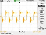
The problem is Why the distortion / Spiking's decreases as current increases?
Can we over come this effect when there is no load?
and why is this happening?

Thank you

Best Regards.
 

Attachments

  • 4.BMP
    76.1 KB · Views: 47

Please consider forum rules about uploaded images:
Avoid using bmp image format, it occupies a huge size compared to the formats described above and can’t be shown directly in a browser which is an additional inconvenience.
You can convert .bmp to .png or .jpg with any graphic tool of you choice, e.g. Irfanview or Windows Paint.

If you look sharp, you'll realize that the load resistance doesn't actually reduce the peak-to-peak ringing magnitude. It only removes the overshoot by adding a low-pass response caused by the transformer leakage inductance. Hence the ringing is hidden in rising edge.

It would be interesting to look at the primary waveform, e.g. bridge center to DC-. Most likely, the ringing already present it the bridge output, caused by parasitic circuit inductance.
 
Ah sorry about the .bmp
next time i will send it as jpg. Also I've the Primary sides figure below

Primary.jpg

it looks the same as in the secondary side (also that figure was taken when there was no current)
Isn't it possible to reduce the effects of parasitic capacities?
or maybe can we reduce these effects by choose a lower Cgs, Cgd, Cds values of mosfet?
 

the whole ckt would be useful to answer your questions, but in short, too open a layout with no nearby bus caps causes the sort of effects you are seeing ...
 
  • Like
Reactions: FvM

    FvM

    Points: 2
    Helpful Answer Positive Rating
Status
Not open for further replies.

Part and Inventory Search

Welcome to EDABoard.com

Sponsor

Back
Top