votientu
Member level 2
Hello,
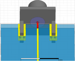
I simulate the SMA model in HFSS (a PCB board which comprises of 2 SMA connectors and a transmission line) and it shows the mismatch problem.
The mismatch does not come from the transmission line nor coaxial transmission in SMA (I verified it) so I suppose it comes from the connection between SMA and the board.
The SMA model is designed to simulate the SMA connector JOHNSON 142-0701-851 (RF / Coaxial Connector, SMA Coaxial) which works up to 18 GHz.
**broken link removed**
I found it is strange that I see the same mismatch in my measurement with this connector. So I wonder if my installation (as I show in the simulation) is not good ?
Should I choose another SMA connector ?
Thanks !


