hg527
Newbie level 5
Hi,everyone:
I use Virtex5 and ISE10.1. I connect one chip’s single ended clock to the N-side of clock capable pins of Virtex5 FPGA by accident on my PCB board. But Xilinx’s manual demands :“1)Do not connect a single ended clock to the N-side of the differential clock pair of pins, for example IO_L3N_GC_3. 2)Do not connect a single-ended clock to the N-side of clock capable pins, for example, IO_L8N_CC_11”. It’s really a tragedy.
However,I use ISE10.1 to place and route my synthesized results and there is no errors reported. Indeed, floorplan show errors as above mentioned.
The world is relative. Clock signal and other signals also are relative. Does it mean some primitives, such as BUFG, PLL_ADV, DCM_ADV, cannot be placed or routed to FPGA chip pad?
My question is :
1) What is the result if I connect a single ended clock tothe N-side of clock capable pins?
2) If it is dangerous or can not implement, How can I do? After all,it is a hardware ‘hurt’.
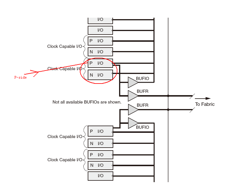
3) What’s the difference between P-side and N-side? Do we have the common sense that P-side is ‘rich’while N-side is ‘poor’? What is the architecture of the IOB?
Do anyone have advice? Who can explain? Thanks forever.
I use Virtex5 and ISE10.1. I connect one chip’s single ended clock to the N-side of clock capable pins of Virtex5 FPGA by accident on my PCB board. But Xilinx’s manual demands :“1)Do not connect a single ended clock to the N-side of the differential clock pair of pins, for example IO_L3N_GC_3. 2)Do not connect a single-ended clock to the N-side of clock capable pins, for example, IO_L8N_CC_11”. It’s really a tragedy.
However,I use ISE10.1 to place and route my synthesized results and there is no errors reported. Indeed, floorplan show errors as above mentioned.
The world is relative. Clock signal and other signals also are relative. Does it mean some primitives, such as BUFG, PLL_ADV, DCM_ADV, cannot be placed or routed to FPGA chip pad?
My question is :
1) What is the result if I connect a single ended clock tothe N-side of clock capable pins?
2) If it is dangerous or can not implement, How can I do? After all,it is a hardware ‘hurt’.
3) What’s the difference between P-side and N-side? Do we have the common sense that P-side is ‘rich’while N-side is ‘poor’? What is the architecture of the IOB?
Do anyone have advice? Who can explain? Thanks forever.