Continue to Site
Follow along with the video below to see how to install our site as a web app on your home screen.
Note: This feature may not be available in some browsers.
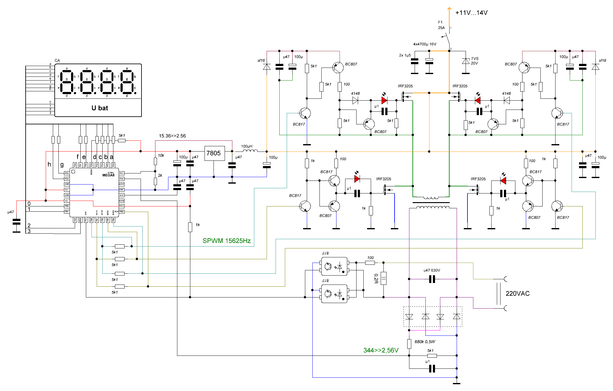
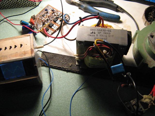
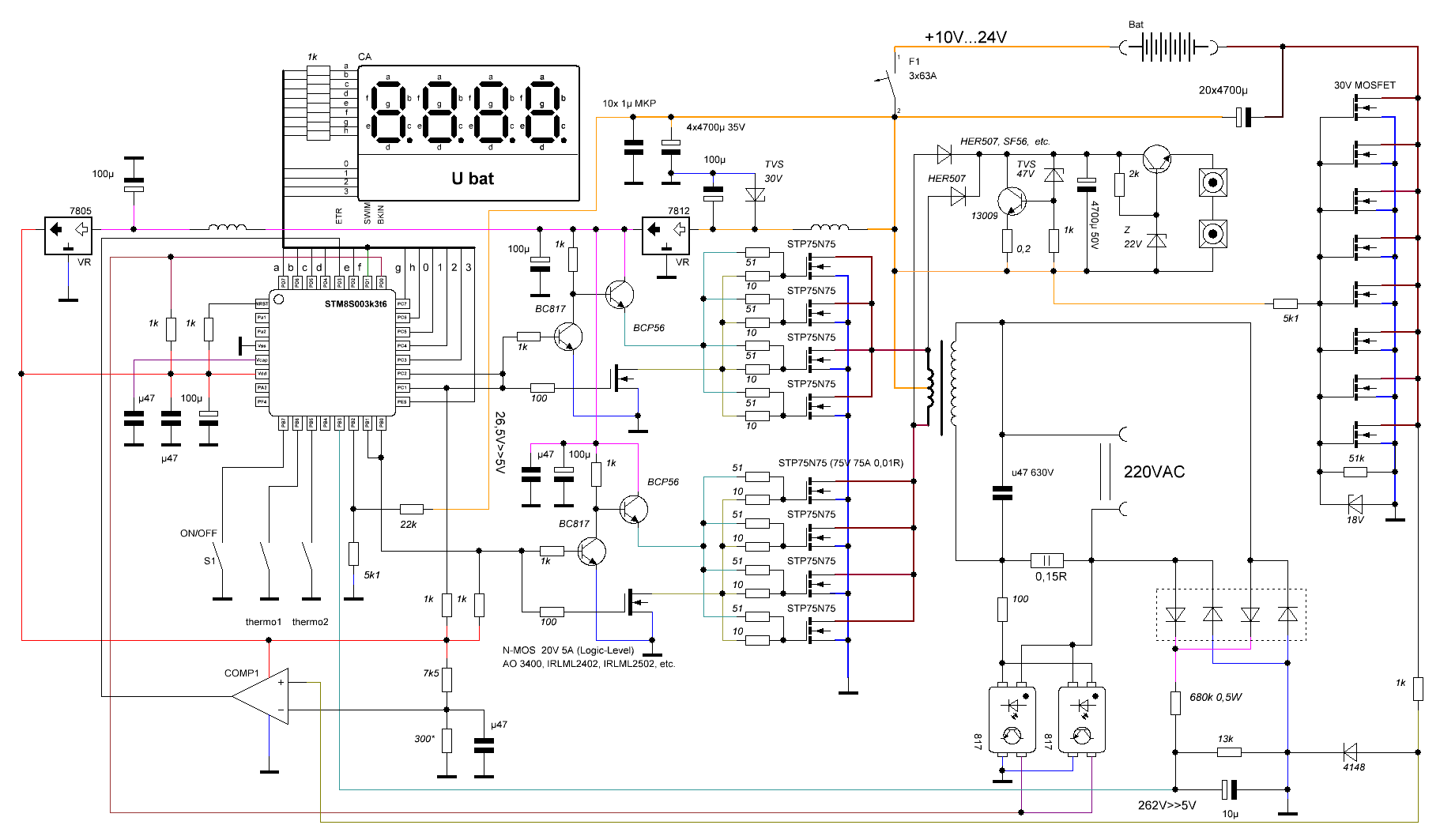
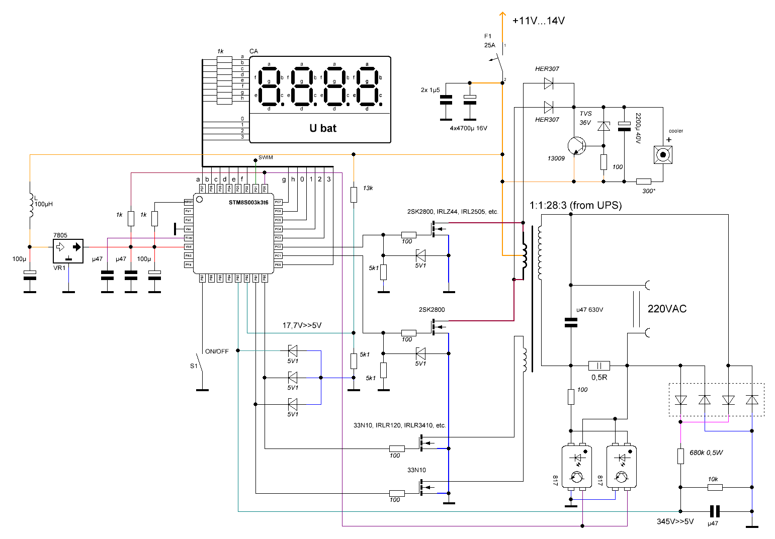
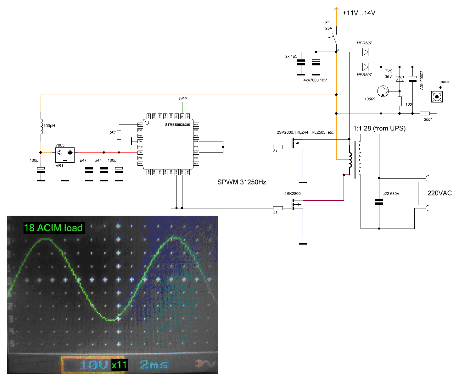
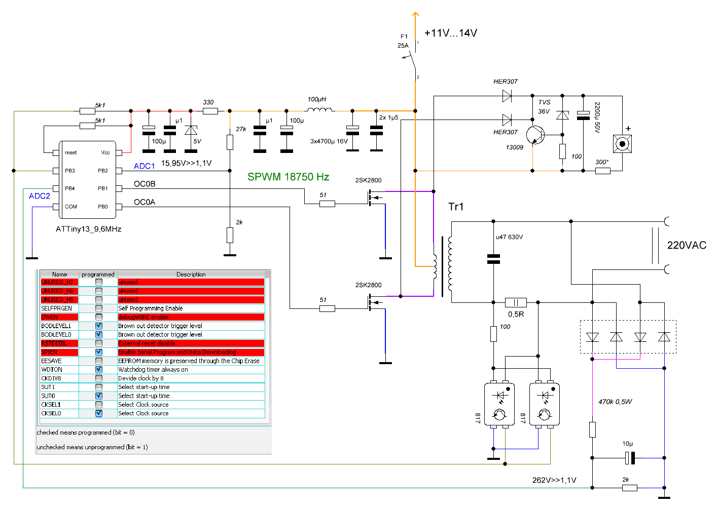
only driver part with stm8 mcuDid you check this last schematic in Hardware?
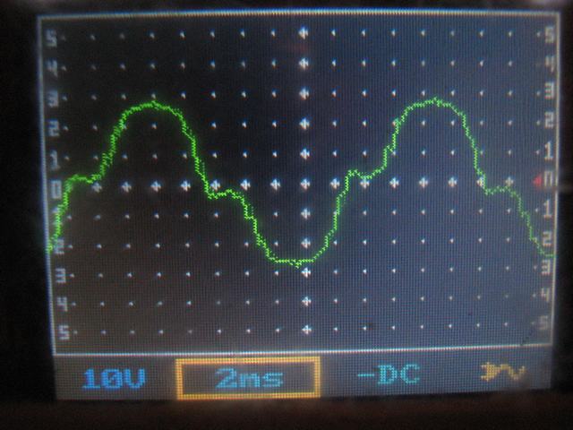
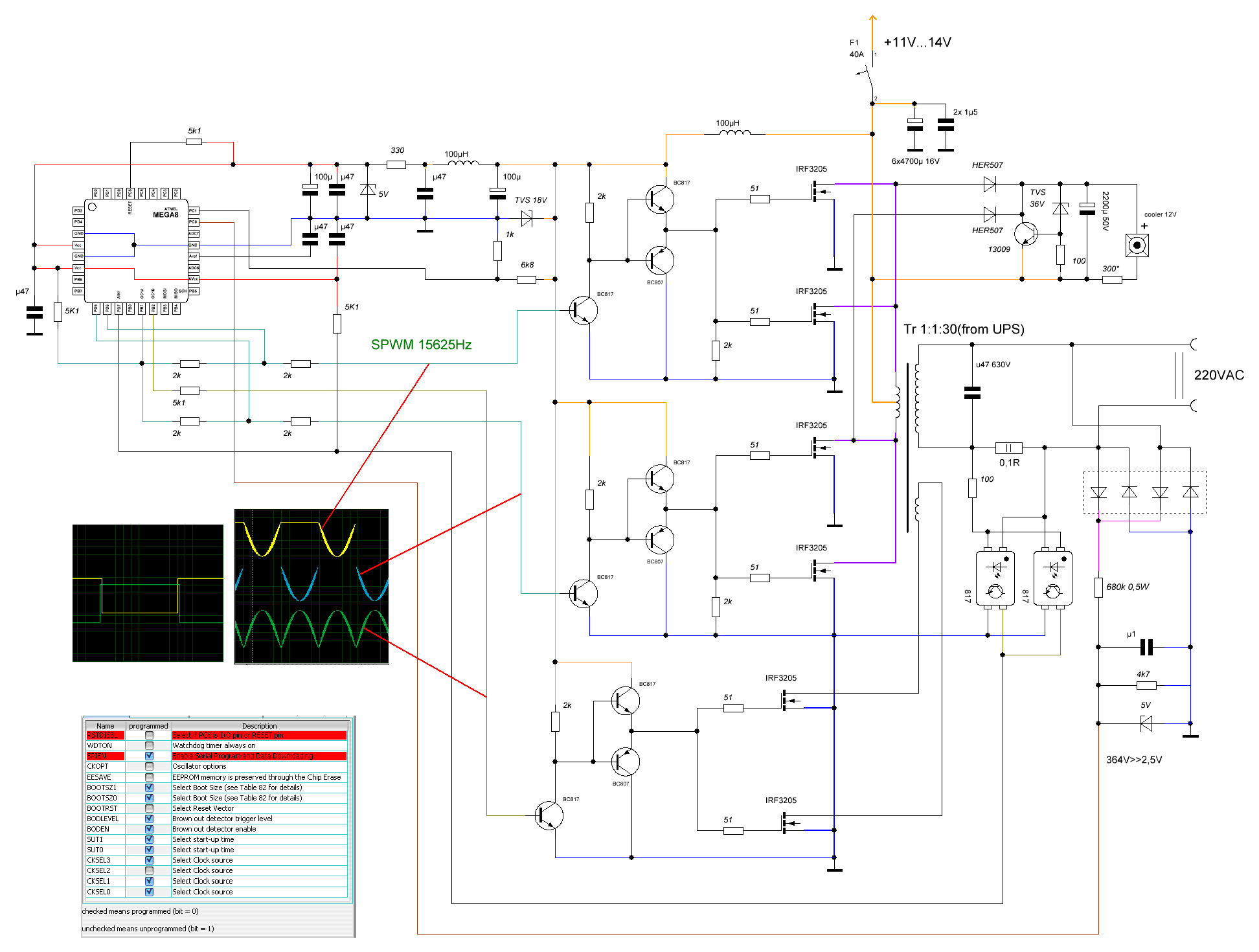
yes, it may work in 50Hz - 30KHz rangeI think this is cheap and will work for 15khz SPWM
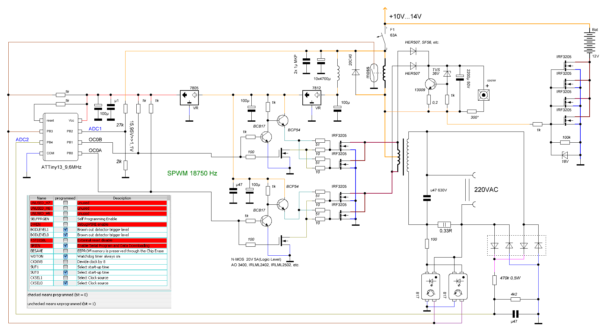
no, it is much worse then with IR2110, because power and hi-side driver signals are too bound.Is this scheme better than IR2110 or any other dedicated chip based bridge.