Continue to Site

Welcome to EDAboard.com

Welcome to our site! EDAboard.com is an international Electronics Discussion Forum focused on EDA software, circuits, schematics, books, theory, papers, asic, pld, 8051, DSP, Network, RF, Analog Design, PCB, Service Manuals... and a whole lot more! To participate you need to register. Registration is free. Click here to register now.

simulation in ltspice

Status
Not open for further replies.

sinan2

Newbie level 4
Joined
May 8, 2017
Messages
5
Helped
0
Reputation
0
Reaction score
0
Trophy points
1
Activity points
51
i tyy to simulate in lt spice ac/dc voltage doubler for electromagnetic harvesting
and i use 2 comparators to control 2 pmos
and those comparators used supply voltage vss and vdd (not external power but self powred from the same source electromagnetic)
the probleme is the 2 sources are inversed vss be vdd and vdd be vss
when i connect them to comparator
maybe in the article he use 2 channel comparator and i work with 2 comparator with 1 channel !!!!!!!!!
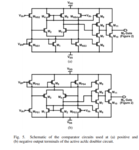
why we use cmos to Schematic of the comparator circuits !!!!
what is the difference betwen normal comparator and the cmos circuit used in comparator !
ddd.PNG
comp.PNG
 

If you are talking ambient RF energy without a nearby
strong source I think those comparators will bleed you
dry.

Take a deep breath, lose a few exclamation points and
try again to explain the problem(s). Some of your questions
or statements don't make sense to me although you
are obviously agitated about something.

The comparators look normal-ish, two different versions
for two different expected input voltage ranges I expect.

Those passive doubler schemes (and the active for that
matter) don't work so well when you have high-VT FETs
and low input signal. There's a "sweet spot" between
no forward conduction, and too much reverse conduction,
that you need to find for any decent RF energy harvesting
when signal power is small.

If you mean to harvest the power to get vdd-vss, and
run the comparators to drive the synchronous rectifier,
that's a chicken/egg kind of scenario, and the egg may
go rotten before you pick up any useful energy.
 

this circuit is a self powred rectifiying electronics for low voltage electromagnetic harvester
and it is combined with piezo source and TE source to have hybrid system to have DC voltage
my input source for Electromagnetic is 0.4v peak to peak with frequency is 35h and input resistance for electromagnetic is 35ohm
this circuit use a passive ccircuit(positive doubler and negative doubler ) to generate VDD and vss to supply voltage to active circuit(pmos and comparator)
when i pick pmos with low threshold voltage and comparator for low power it dosen't work
and when i simulate the positive and negative supply voltage they inversed VSS go to positive and vdd go t negative
 

Try starting with just the doubler-pump switch PMOS
devices, and ideal (pulse source) gate drive, and the
RF input "stimulus". Figure out what gate drive signal
pair optimizes the harvested voltage, and compare this
(heh) to the comparators' behaviors. Maybe the two
comparator positions want the opposite type (input
working range, vs startup and operating common mode
voltage conditions, etc. - both types will have their
front end cut off, just at different ends of the vss-vdd
input range.

Cut the problem apart, and stitch it back together
once you have working pieces.
 

Status
Not open for further replies.

Similar threads

Part and Inventory Search

Welcome to EDABoard.com

Sponsor

Back
Top