Continue to Site

Welcome to EDAboard.com

Welcome to our site! EDAboard.com is an international Electronics Discussion Forum focused on EDA software, circuits, schematics, books, theory, papers, asic, pld, 8051, DSP, Network, RF, Analog Design, PCB, Service Manuals... and a whole lot more! To participate you need to register. Registration is free. Click here to register now.

Simple Mosfet design advice / assistence

Status
Not open for further replies.

dimBulb

Newbie level 2
Joined
Mar 11, 2011
Messages
2
Helped
0
Reputation
0
Reaction score
0
Trophy points
1,281
Activity points
1,316
Hello,
I'm looking to switch a 10~30V load at up to 5A from a 3.3V microcontroller.
Driving a low side logic level N-Channel Mosfet directly from the 3.3V functions but the mosfet burns out if the switching speed gets much faster than 5K, lack of voltage and charge current. I'd like to acheive on/off speeds around 100-200ns.

I've considered a few options and would really like to know what the common approach is for this sort of situation.
1) Change to High-Side P-Channel and use a transistor to bring the gate towards ground. Gives me a bit higher RDS and I need additional measures to try and keep the gate from exceeding -20V when the supply is 20V+. Zener clipping circuit perhaps?
2) Intelligent Power Switches - would be fantastic but don't have the desired switching speeds, and costs do seem a bit high.
3) Use a mosfet driver. Most have a vcc limit below my supply limit and I'm hoping not to have to run another supply level. Application has potential for 100% on time so bootstrapping wouldn't work.

Throwing on another regulator and using a driver may be the easiest option.
Is there another alternative I'm not considering?
Is running a gate level supply common place in this sort of design?
High-side / low-side / N-Channel / P-Channel, I'm not really stuck on any of them, I'd like to keep the costs and component count down though.

Thanks In Advance.
Your solution is not very simple. First a buffer is needed to amplify the output of the processor to drive the gate of the fet. The current needed to drive the gate of the fet at 100ns equals ( I = C x ( 12/100ns )). The C is the total gate charge. Also the load, if it is inductive, will need to be snubbed or clamped to reduce the avalanch energy. A fast diode may be the answer. In the formula the 12 is the typical voltage required by most n channel inhansment power mosfets. The processor output of 3.3v is the other reason a buffer is needed to be increased to 12 volts. Also the fet must be driven on as well as off with similar currents depending upon what the load happens to be.
I hope this is some help.
Yar.
 

The current needed to drive the gate of the fet at 100ns equals ( I = C x ( 12/100ns )). The C is the total gate charge. Also the load, if it is inductive, will need to be snubbed or clamped to reduce the avalanch energy. A fast diode may be the answer. In the formula the 12 is the typical voltage required by most n channel inhansment power mosfets.

I have never seen the voltage be used in a calculation like this,
a total gate charge of Qg=20nC means that the mosfet will be fully on in 20ns with 1A gate current (or 40ns with 0.5A etc),
for 100ns you should use I=Qg/100ns (Qg in ns and I in amps), the gate voltage has nothing to do with that calculation assuming that it is above the gate threshold voltage

Alex

Alex,

The 12v is needed if a larger low cost avaliable mosfet is required because of the overheating mentioned earlier. Most of these are driven with 12v. Otherwise you are correct concerning the risetime and current required. The buffer is still needed to covert the processor output current to that of the fet requirement for a given risetime. Such as the IR4426 or the older ds0026.

Yar
 

My only objection was for the gate voltage used in the calculation of the switcing speed, nothing else.
Yes the voltage should be high enough (based on the needs of each specific mosfet) to give a low Rds-on,
also a level translator is needed to provide the proper voltage level and also a driver stage to sink/source the high current of the gate.

Alex

Sorry Alex,
I missunderstood. The correct calcs are using the load voltage needed to switch such as 30 volts and using the Crss of the fet as "C" then the needed gate drive current I is ( I= Crss ( 30 volts/ 200ns )) this gives the exact current needed to switch during the plateau period seen on the data sheet of the fet. At this time no current is driven into the Ciss of the fet.
Yar.
 

Thank You for the responses.
I currently have two available supplies a 3.3V logic supply and a system supply that will be between 10-30VDC. I know I need a gate drive circiut. What I'm curious on is what the common practice is in handling the level shift requirements for the gate, since most of the fet's I've looked at N or P have between a 20 ~ 25V VGS maximum, there are some 30V ones but tend to be a bit costly. If Vs is 30V the driver will power the gate at 30V exceeding the maximum VGS, correct? Changing topology a bit and running a pchannel high side and driving it to ground to enable the circuit would exceed VGS once again at the high end of the supply.

Thanks again.
 

Hi,
I understand you have 3.3 volts and the 10 to 35 volt power supply but some how you need 12volts to drive the power fet. A three terminal regulator is a good way to get the 12 volts from the 35v supply but this is too close to the maximum limit of the regulators without adding a zener diode in series with the regulator but this will not work with the input at 10 volts. The best way is to use a 12 volt zener diode with a 3k series resistor as below ( with a npn transistor ) the output of 8.8 to 12v will drive most power mos fets with a buffer.
I can not attach a sketch of a suggested circuit.
Yar
 
Last edited:

You can try a solution like

Nmosfet_driver.jpg

This includes a level translator with a 330/(330+560) ratio which gives about 11v (30v*0.37) with 30v power supply,
then a totem pole driver is used to source/sink the gate charge/discharge current fast so that the mosfet doesn't overheat (fast on/off transition).
The level translator collector resistance adjusts the amount of current going to the base of the totem pole driver so the values may need to be lower (same analogy to keep the ratio) depending on the hfe of the transistors used.

Alex
 

… The current needed to drive the gate of the fet at 100ns equals ( I = C x ( 12/100ns )). The C is the total gate charge.

Yar probably meant "C is the total gate capacitance".

I have never seen the voltage be used in a calculation like this, ...

In this case the incorporation of the Δ(Vgs) of 12V is correct of course: Qg = C x Δ(Vgs) .


... you should use I=Qg/100ns (Qg in ns and I in amps), ...

Qg in As of course.
 

Qg is the total gate charge and is given in nC, (I wrote ns by mistake),
because i use nano seconds in the above calculation I also wrote that the Qg should be used in nC (ns by mistake) and I in amps (the result).

What so you mean by

Qg in As of course


Qg in amperes?

Alex
 
  • Like
Reactions: Yar

    Yar

    Points: 2
    Helpful Answer Positive Rating
Alex,

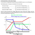
The rise time of the on or off of the fet gate drive is a function of the crss only. the Crss and ciss add up to be the total gate charge. The proff can be seen on the fets data sheet of the Vgs vs Qg. You will see a plateau in this curve. There is no current in the Ciss. All of the gate drive current is in the Crss. This is the time the fet is switching. The rise time ( c x v)= ( I x t ) of the fet which is exactly the gate drive current = I. The C = the Crss. The V = voltage being switched. The t = fall time of the fet switching.
Yar
 

@erikl
You are probably more experienced in the theory behind this than i am but i wasn't aware of As,
Qg is always given in nC (which involves current * time ) but i have never seen it called As

In the calculation i wrote in the previous post i was using I=Qg/100ns (Qg in nC and I in amps),
time is 100ns so the gate charge should be also used in nano so that the result is amperes,
if you write the Qg as Amperes x seconds then the result would be nA not Amperes.


@Yar
So when you calculate the gate current you should give to achieve a switching rate you say that the Qg doesn't matter?
What about the switching losses, as long as the mosfet can switch on/off losses don't matter?

Attached image source https://www.fairchildsemi.com/an/AN/AN-9010.pdf (page 17)

Alex

UPDATE: erikl meant nAs (which is the same as nC) and not As as I originally thought, so his suggestion was correct.
 

Attachments

  • Mosfer_gate_charge.jpg
    Mosfer_gate_charge.jpg
    90.5 KB · Views: 149
Last edited:
  • Like
Reactions: Yar

    Yar

    Points: 2
    Helpful Answer Positive Rating
Alex,
This attachment is nearly correct. The Crss has some change in value due to the vari-cap effect but my views are almost a straight line ( during the plateau period) with a very small curve when the Vds is almost fully turned on.
Yar
 

Status
Not open for further replies.

Similar threads

Part and Inventory Search

Welcome to EDABoard.com

Sponsor

Back
Top