Continue to Site

Welcome to EDAboard.com

Welcome to our site! EDAboard.com is an international Electronics Discussion Forum focused on EDA software, circuits, schematics, books, theory, papers, asic, pld, 8051, DSP, Network, RF, Analog Design, PCB, Service Manuals... and a whole lot more! To participate you need to register. Registration is free. Click here to register now.

Signal description of GTH transceivers

engr_joni_ee

Advanced Member level 3
Joined
Nov 3, 2018
Messages
750
Helped
2
Reputation
4
Reaction score
4
Trophy points
18
Activity points
6,229
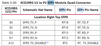
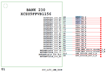
How we describe the signal between FPGA and SFP+ connector on the PCB traces. There are two differential pairs in SFP+ connector, one for Tx and the other is for Rx. What is the clock frequency and clock period of Tx and Rx signals between FPGA and SFP+ connector on the PCB traces ? If someone need to draw the waveform for understanding then which frequency and voltage level to use.
 

Attachments

  • Untitled 295.png
    Untitled 295.png
    29.2 KB · Views: 67
  • Untitled 296.png
    Untitled 296.png
    86.5 KB · Views: 68
Hi again,

I have looked at the datasheet of SFP+ which says that it support 10 G Ethernet and 10 G Fiber.

There are five signals in SFP+ connector PCB mount.

SFP0_TX_P/N
SFP0_RX_P/N
SFP0_TX_DISABLE

There are only two differential pairs (one Tx differential pair and the one Rx differential pair) and one Tx disable signal. All five signals has to be connected to ZYNQ UltraScale+ MPSoC on PL side. All the data (10 G) is transmitted and received through these two differential pairs, right ? I am interested to know their waveform. The datasheet says about rise time (30 ps) and fall time (30 ps) but this is not sufficient to draw the waveform with time period and amplitude showing 10 G data transfer. How can I get this information ?

Again, all the data (10 G) is transmitted and received through these two differential pairs or some other signals also contain data between PCB mount SFP+and ZYNQ UltraScale+ MPSoC ?
 
The datasheet specifies levels and signal rate, what do you need else to sketch a waveform?
Yes, TX and Rx are 10 GBPS differential signals. For coding details, you can refer to the 10G section of IEEE 802.3 or internet sources.

Or review Xilinx 10G Ethernet IP doc https://docs.xilinx.com/v/u/en-US/pg068-ten-gig-eth-pcs-pma.
 
Thanks for sharing the document. I will look into the document and try to understand the signaling and coding at physical layer how we get 10 GBPS with TX and Rx differential signals.
 
I am concerned with PCB design and that's why I am interested to know the signal in physical layer. Do I need to know coding ? I don't think so. I am interested in wire speed of differential pair. If 10 Gbits/s is duplex, meaning each way is 10 Gbits/s then the clock frequency of differential siganls Tx or Rx should be 5 GHz sampling at both edges, right ? I saw in the Xilinx high speed serial transceivers where it shows 200 ps width of a period which is 5 GHz clock frequency. Is that really 5 GHz clock frequency differential signals between PCB mount SFP+and ZYNQ UltraScale+ MPSoC ? If yes, then what are the length of trace limitations ?
 

LaTeX Commands Quick-Menu:

Similar threads

Part and Inventory Search

Welcome to EDABoard.com

Sponsor

Back
Top