Continue to Site

Welcome to EDAboard.com

Welcome to our site! EDAboard.com is an international Electronics Discussion Forum focused on EDA software, circuits, schematics, books, theory, papers, asic, pld, 8051, DSP, Network, RF, Analog Design, PCB, Service Manuals... and a whole lot more! To participate you need to register. Registration is free. Click here to register now.

Seven-Segment Display Driver Chip with shift register (verilog)

Status
Not open for further replies.

lylemalone

Newbie level 1
Joined
Apr 9, 2014
Messages
1
Helped
0
Reputation
0
Reaction score
0
Trophy points
1
Activity points
13
Hi all, I'm a beginner when it comes to verilog and I'm hoping to get some feedback on a project I'm working on:

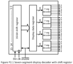
Description: The circuit block diagram that can display four seven-segment displays with a shift register and a display buffer is shown in Figure P2.1. When the enable signal is low, the data to be displayed can be shifted in from the Din pin. When the enable signal goes high, the data cannot be shifted in. On the rising edge of the enable signal, the display data is transferred to the display data register and update the four seven-segment displays. The most significant bit is shifted in first.
Capture.PNG

Below is the code I've come up with. I hope I made a solid approach at this but I'm not sure and can't test it at the moment. The way i split the sixteen bits on the shift register into each of the four decoders seemed simple enough, but i feel like perhaps I oversimplified the problem?

Code:
module bcd_to_seven_seg(bcd1,bcd2,bcd3,bcd4,din,clk,enable, qout);
    output reg [3:0] bcd1, bcd2, bcd3, bcd4; //declaring each 4-bit decoder
    input din, clk, enable;
    output reg [15:0] qout; //shift register values

    always @(posedge clk && !enable) begin //start shifting register on 
        qout[0] = qout[1];                 //on positive clock edge and 
        qout[1] = qout[2];                 // when enable is low
        qout[2] = qout[3];
        qout[3] = qout[4];
        qout[4] = qout[5];
        qout[5] = qout[6];
        qout[6] = qout[7];
        qout[7] = qout[8];
        qout[8] = qout[9];
        qout[9] = qout[10];
        qout[10] = qout[11];
        qout[11] = qout[12];
        qout[12] = qout[13];
        qout[13] = qout[14];
        qout[14] = qout[15];
        qout[15] = din;
    end

    always @(posedge enable) begin      //transfer data to decoders on
        bcd1[3] = qout[15];             //enable's positive edge
        bcd2[3] = qout[11];
        bcd3[3] = qout[7];
        bcd4[3] = qout[3];
        bcd1[2] = qout[14];
        bcd2[2] = qout[10];
        bcd3[2] = qout[6];
        bcd4[2] = qout[2];
        bcd1[1] = qout[13];
        bcd2[1] = qout[9];
        bcd3[1] = qout[5];
        bcd4[1] = qout[1];
        bcd1[0] = qout[12];
        bcd2[0] = qout[8];
        bcd3[0] = qout[4];
        bcd4[0] = qout[0];
    end

    always @(bcd1 | bcd2 | bcd3 | bcd4) begin
        case (bcd1)
            0: bcd1 = 7'b0111111;
            1: bcd1 = 7'b0000110;
            2: bcd1 = 7'b1011011;
            3: bcd1 = 7'b1001111;
            4: bcd1 = 7'b1100110;
            5: bcd1 = 7'b1101101;
            6: bcd1 = 7'b1111101;
            7: bcd1 = 7'b0000111;
            8: bcd1 = 7'b1111111;
            9: bcd1 = 7'b1101111;
            default: bcd1 = 7'b0000000;
        endcase   
        
        case (bcd2)
            0: bcd2 = 7'b0111111;
            1: bcd2 = 7'b0000110;
            2: bcd2 = 7'b1011011;
            3: bcd2 = 7'b1001111;
            4: bcd2 = 7'b1100110;
            5: bcd2 = 7'b1101101;
            6: bcd2 = 7'b1111101;
            7: bcd2 = 7'b0000111;
            8: bcd2 = 7'b1111111;
            9: bcd2 = 7'b1101111;
            default: bcd2 = 7'b0000000;
        endcase
        
        case (bcd3)
            0: bcd3 = 7'b0111111;
            1: bcd3 = 7'b0000110;
            2: bcd3 = 7'b1011011;
            3: bcd3 = 7'b1001111;
            4: bcd3 = 7'b1100110;
            5: bcd3 = 7'b1101101;
            6: bcd3 = 7'b1111101;
            7: bcd3 = 7'b0000111;
            8: bcd3 = 7'b1111111;
            9: bcd3 = 7'b1101111;
            default: bcd3 = 7'b0000000;
        endcase
    
        case (bcd4)
            0: bcd4 = 7'b0111111;
            1: bcd4 = 7'b0000110;
            2: bcd4 = 7'b1011011;
            3: bcd4 = 7'b1001111;
            4: bcd4 = 7'b1100110;
            5: bcd4 = 7'b1101101;
            6: bcd4 = 7'b1111101;
            7: bcd4 = 7'b0000111;
            8: bcd4 = 7'b1111111;
            9: bcd4 = 7'b1101111;
            default: bcd4 = 7'b0000000;
        endcase
    end
endmodule
 

lylemalone,

I'll throw in a couple of quick suggestions, and the community will probably throw in several more good ones:

1) in your sensitivity list, make sure the edge event always blocks do not have unnecessary signals
2) it is best practive to put non-blocking statements in edge-triggered circuits.
3) it is nice to have reset conditions built into edge-triggered circuits, but not necessary.

Code:
always @(posedge clk && !enable) begin //start shifting register on 
        qout[0] = qout[1];                 //on positive clock edge and 
        qout[1] = qout[2];                 // when enable is low
        qout[2] = qout[3];
        qout[3] = qout[4];
        qout[4] = qout[5];
        qout[5] = qout[6];
        qout[6] = qout[7];
        qout[7] = qout[8];
        qout[8] = qout[9];
        qout[9] = qout[10];
        qout[10] = qout[11];
        qout[11] = qout[12];
        qout[12] = qout[13];
        qout[13] = qout[14];
        qout[14] = qout[15];
        qout[15] = din;
    end
    

    //no reset
    always @(posedge clk) 
    begin 
        if(~enable)
        begin
            qout[0] <= qout[1];                 
            qout[1] <= qout[2];                
            qout[2] <= qout[3];
            qout[3] <= qout[4];
            qout[4] <= qout[5];
            qout[5] <= qout[6];
            qout[6] <= qout[7];
            qout[7] <= qout[8];
            qout[8] <= qout[9];
            qout[9] <= qout[10];
            qout[10] <= qout[11];
            qout[11] <= qout[12];
            qout[12] <= qout[13];
            qout[13] <= qout[14];
            qout[14] <= qout[15];
            qout[15] <= din;
        end
    end

//async reset included
 always @(posedge clk, posedge reset) 
    begin 
        if(reset)
        begin
            qout    <= 16'h0000;
        end
        else if(~enable)
        begin
            qout[0] <= qout[1];                 
            qout[1] <= qout[2];                
            qout[2] <= qout[3];
            qout[3] <= qout[4];
            qout[4] <= qout[5];
            qout[5] <= qout[6];
            qout[6] <= qout[7];
            qout[7] <= qout[8];
            qout[8] <= qout[9];
            qout[9] <= qout[10];
            qout[10] <= qout[11];
            qout[11] <= qout[12];
            qout[12] <= qout[13];
            qout[13] <= qout[14];
            qout[14] <= qout[15];
            qout[15] <= din;
        end
        else
        begin
            qout    <= qout;
        end
    end
 

You've got numerous problems in this code.

Not a problem but easier to maintain...Use Verilog 2001 C-syntax for the module ports:

Code Verilog - [expand]
1
2
3
4
5
module bcd_to_seven_seg (
  output reg [3:0]  bcd1, bcd2, bcd3, bcd4, //declaring each 4-bit decoder
  input             din, clk, enable,
  output reg [15:0] qout  //shift register values
);


I normally have only one port per line too, but then I usually have a comment on each port.

You are right shifting MSB to LSB when you said the requirement was to shift out the MSB first?
The most significant bit is shifted in first
This is how you should write a shift operation.

Code Verilog - [expand]
1
2
qout <= {qout[14:0, din}; // this is a left shift, shifting from LSB to MSB
qout <= {din, qout[15:1]}; // this is a right shift, shifting from MSB to LSB


You are not using a standard template for a register with enable. This code won't synthesize correctly.

Code Verilog - [expand]
1
2
3
4
5
6
7
8
9
10
11
12
13
14
15
16
17
18
always @(posedge clk && !enable) begin //start shifting register on 
        qout[0] = qout[1];                 //on positive clock edge and 
        qout[1] = qout[2];                 // when enable is low
        qout[2] = qout[3];
        qout[3] = qout[4];
        qout[4] = qout[5];
        qout[5] = qout[6];
        qout[6] = qout[7];
        qout[7] = qout[8];
        qout[8] = qout[9];
        qout[9] = qout[10];
        qout[10] = qout[11];
        qout[11] = qout[12];
        qout[12] = qout[13];
        qout[13] = qout[14];
        qout[14] = qout[15];
        qout[15] = din;
    end

This is the standard template for a register with a synchronous enable.

Code Verilog - [expand]
1
2
3
4
5
always @ (posedge clk) begin
  if (!enable) begin
    // your enabled code goes here
  end
end


You are using blocking assignments in a clock always block, which won't synthesize correctly and will result in a mismatch between simulation and synthesis.

Code Verilog - [expand]
1
2
qout[0] = qout[1];  // blocking assignment, do not use in a clocked always block
qout[0] <= qout[1];  // non-blocking assignment, this is the correct way to code a register in a clocked always block


You are creating clock from an internal register, this is a poor design practice.

Code Verilog - [expand]
1
always @(posedge enable) begin      //transfer data to decoders on

Instead you should synchronously edge detect the enable and use that to perform a load.

I'm not even sure what this is supposed to be.

Code Verilog - [expand]
1
2
3
4
5
6
7
8
9
10
11
12
13
14
15
16
17
18
19
20
21
22
23
24
25
26
27
28
29
30
31
32
33
34
35
36
37
38
39
40
41
42
43
44
45
46
47
48
49
50
51
52
53
54
55
56
57
always @(bcd1 | bcd2 | bcd3 | bcd4) begin
        case (bcd1)
            0: bcd1 = 7'b0111111;
            1: bcd1 = 7'b0000110;
            2: bcd1 = 7'b1011011;
            3: bcd1 = 7'b1001111;
            4: bcd1 = 7'b1100110;
            5: bcd1 = 7'b1101101;
            6: bcd1 = 7'b1111101;
            7: bcd1 = 7'b0000111;
            8: bcd1 = 7'b1111111;
            9: bcd1 = 7'b1101111;
            default: bcd1 = 7'b0000000;
        endcase   
        
        case (bcd2)
            0: bcd2 = 7'b0111111;
            1: bcd2 = 7'b0000110;
            2: bcd2 = 7'b1011011;
            3: bcd2 = 7'b1001111;
            4: bcd2 = 7'b1100110;
            5: bcd2 = 7'b1101101;
            6: bcd2 = 7'b1111101;
            7: bcd2 = 7'b0000111;
            8: bcd2 = 7'b1111111;
            9: bcd2 = 7'b1101111;
            default: bcd2 = 7'b0000000;
        endcase
        
        case (bcd3)
            0: bcd3 = 7'b0111111;
            1: bcd3 = 7'b0000110;
            2: bcd3 = 7'b1011011;
            3: bcd3 = 7'b1001111;
            4: bcd3 = 7'b1100110;
            5: bcd3 = 7'b1101101;
            6: bcd3 = 7'b1111101;
            7: bcd3 = 7'b0000111;
            8: bcd3 = 7'b1111111;
            9: bcd3 = 7'b1101111;
            default: bcd3 = 7'b0000000;
        endcase
    
        case (bcd4)
            0: bcd4 = 7'b0111111;
            1: bcd4 = 7'b0000110;
            2: bcd4 = 7'b1011011;
            3: bcd4 = 7'b1001111;
            4: bcd4 = 7'b1100110;
            5: bcd4 = 7'b1101101;
            6: bcd4 = 7'b1111101;
            7: bcd4 = 7'b0000111;
            8: bcd4 = 7'b1111111;
            9: bcd4 = 7'b1101111;
            default: bcd4 = 7'b0000000;
        endcase
    end

I think you are trying to convert the bcd1 - bcd4 values to the equivalent seven segment control output, but don't seem to understand what that means. You should have captured the shifted values in another signal like binary_capture.

Code Verilog - [expand]
1
2
3
4
5
6
7
8
9
10
binary_capture <= load ? qout : binary_capture; // load is the synchronous rising edge detector of the enable signal.
 
case (binary_capture[15:12])
  0: bcd1 <= 7'b0111111;
  1: bcd1 <= 7'b0000110;
  // ...
  9: bcd1 <= 7'b1101111;
  default: bcd1 <= 7'b0000000; // defaults is all off or perhaps make it look like an E.
endcase\
// you'll do the same for binary_capture[11:8], etc


I also think the bcd1 - bcd4 outputs should be registered so it won't have glitches, which would cause visible garbage as it switches between numbers.

Regards
 
Last edited:

Status
Not open for further replies.

Part and Inventory Search

Welcome to EDABoard.com

Sponsor

Back
Top