FlyingDutch
Advanced Member level 1
- Joined
- Dec 16, 2017
- Messages
- 457
- Helped
- 45
- Reputation
- 92
- Reaction score
- 55
- Trophy points
- 28
- Location
- Bydgoszcz - Poland
- Activity points
- 4,958
Hello, forum,
some time ago I published a post related to the FPGA board based on the Gowin GW1N-LV9LQ144C6/I5 chip. See post:
 www.edaboard.com
I ordered PCB in JLCPCB and then mounted the prototype. I checked this FPGA board with some FPGA projects and all hardware components are working properly (I also checked PSRAM and external Flash). There was a FTDI USB programer for the FPGA chip and it also work fine with "Gowin Programmer". After checking all components I implemented NEORV32 (RISC-V) soft-cpu on this board and it worked fine. See the link to the project:
https://github.com/stnolting/neorv32
The second edition of PCB has been designed. This version is more professional - some things has been improved:
1) Power planes
2) All high-speed signals and differential pairs of I/O pin traces are designed with length-matching
3) the size of the PCB is smaller
4) PCB has been designed for small EMI emission
This board is well-equipped with peripherals and has 64 I/O pins lead-out for headers. Every I/O bank can be powered by 3.3V , 2.5V, 1.2V voltages.
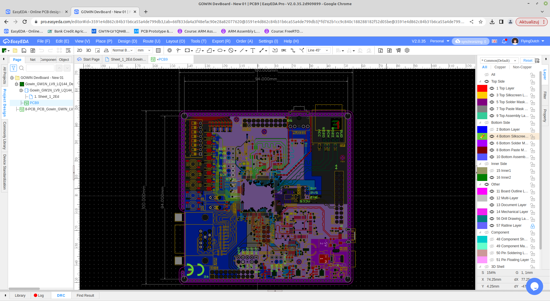
Here is screenshot from EasyEDA Pro CAD:

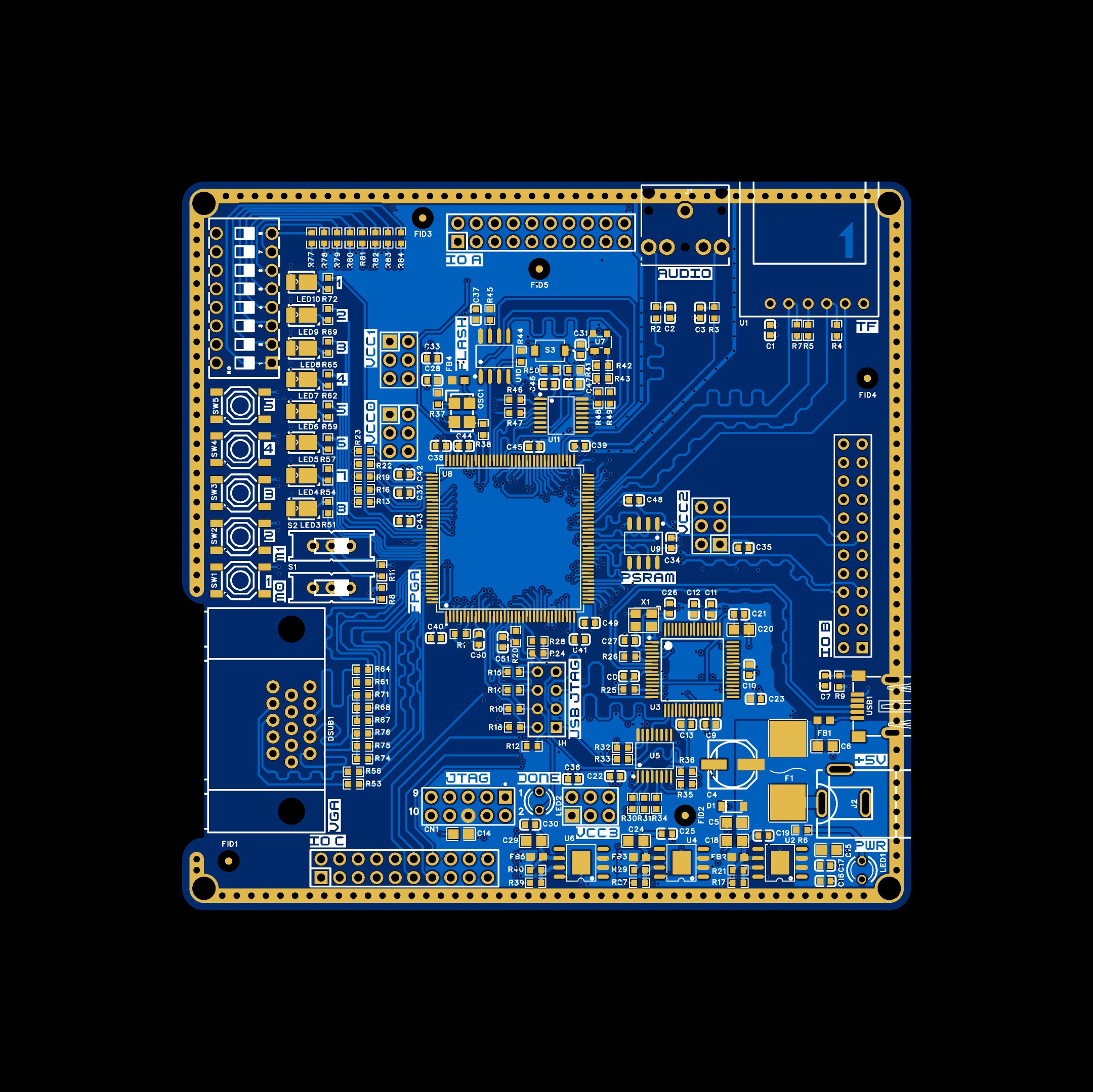
And here is 2D image of board:

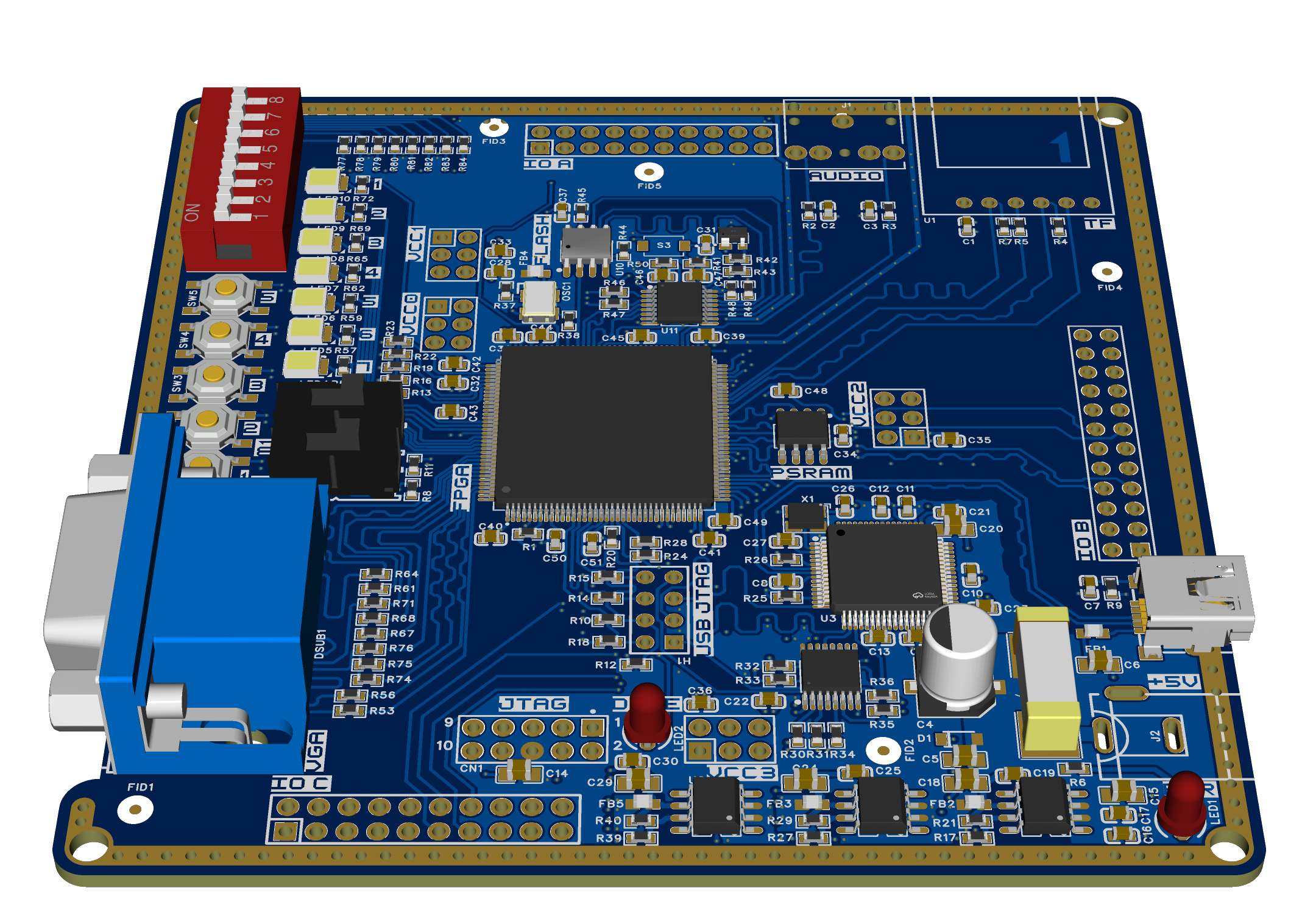
3D image of teh FPGA board:

Regards
some time ago I published a post related to the FPGA board based on the Gowin GW1N-LV9LQ144C6/I5 chip. See post:
Development board with FPGA GW1N-LV9LQ144C6/I5
Hello forum, I designed a simple development board with FPGA from GowinSemi - IC model: GW1N-LV9LQ144C6/I5. Here is link to mouser.com with this product: https://www.mouser.com/ProductDetail/GOWIN-Semiconductor/GW1N-LV9LQ144C6-I5?qs=wnTfsH77Xs6N%2FyGezJZrJQ%3D%3D...
I ordered PCB in JLCPCB and then mounted the prototype. I checked this FPGA board with some FPGA projects and all hardware components are working properly (I also checked PSRAM and external Flash). There was a FTDI USB programer for the FPGA chip and it also work fine with "Gowin Programmer". After checking all components I implemented NEORV32 (RISC-V) soft-cpu on this board and it worked fine. See the link to the project:
https://github.com/stnolting/neorv32
The second edition of PCB has been designed. This version is more professional - some things has been improved:
1) Power planes
2) All high-speed signals and differential pairs of I/O pin traces are designed with length-matching
3) the size of the PCB is smaller
4) PCB has been designed for small EMI emission
This board is well-equipped with peripherals and has 64 I/O pins lead-out for headers. Every I/O bank can be powered by 3.3V , 2.5V, 1.2V voltages.
Here is screenshot from EasyEDA Pro CAD:
And here is 2D image of board:
3D image of teh FPGA board:
Regards