Continue to Site

Welcome to EDAboard.com

Welcome to our site! EDAboard.com is an international Electronics Discussion Forum focused on EDA software, circuits, schematics, books, theory, papers, asic, pld, 8051, DSP, Network, RF, Analog Design, PCB, Service Manuals... and a whole lot more! To participate you need to register. Registration is free. Click here to register now.

Settling time issue in fully differential opamp

Status
Not open for further replies.

bharat_tangudu

Member level 1
Joined
Dec 24, 2015
Messages
40
Helped
0
Reputation
0
Reaction score
0
Trophy points
6
Activity points
423
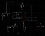
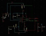
I have designed two-stage fully differential opamp. I took the results and seems every parameter is giving good results except settling time (I believe). To check this, I connected in unity gain configuration and applied the pulse input of 500us (probably, I may be wrong in circuit setup). output is not settling when i run the circuit. Can someone suggest me what to do if settling time has gone worst.

If settling time is not the parameter because of which opamp is giving improper results, can somebody clarify me which one is causing the distortion in output.

Gain 89.5531dB
3dB frequency 903.82Hz
Phase Margin 72.29degrees
Unity Gain bandwidth 45.19MHz
Current in output branch 40.47uA
Bias current 20uA

I am attaching the setup for unity gain amplifier, output
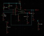
unitygain_setup.jpg

transient_response.jpg

opamp.jpg
 

Re: settling time issue in fully differential opamp

Hi,
It might be a common mode oscillation, and the cause might be the common mode loop.
 

Re: settling time issue in fully differential opamp

Hi ZoOneR,

Are you suggesting me to redesign the common mode feedback network? Can I get the proper explanation for your answer?
 

Re: settling time issue in fully differential opamp

Hi,
Before you change anything you need to check it the cmfb is the problem. You can do a stb analysis to see if the cmfb loop has a propper phase margin.
 

Re: settling time issue in fully differential opamp

If settling time is not the parameter because of which opamp is giving improper results ...

I think you might need feedBack from both outputs, i.e. from o1 to i1, too. Then you'd have to decouple your stimulation source V2 by a cap.

Your V2 input step is too large for your ICMR. Reduce it to about ⅓ or ¼ of the operating voltage.


Re: settling time issue in fully differential opamp

Hi,
Before you change anything you need to check it the cmfb is the problem. You can do a stb analysis to see if the cmfb loop has a propper phase margin.

Thanks for the reply....

I have simulated the amplifier in CMFB network separately and seen the AC response which is giving sufficient phase margin (approximately 90 degrees) to say that this part is stable. However, when I connect this CMFB part in unity gain configuration, the output is not reaching the final state in transient analysisi. I don't know if this is the reason. I am attaching the both AC and transient responses.

transient_response_CMFB.jpg

AC_response_CMFB.jpg

- - - Updated - - -

Thanks for the reply frankrose

There is no unity-gain buffer configuration for full differential amplifiers. You have to use feedback on both sides and test settling time with inverting amplifier configuration.


I haven't seen any document relevant to this statement. can I get any link which supports your sentence?

- - - Updated - - -

I think you might need feedBack from both outputs, i.e. from o1 to i1, too. Then you'd have to decouple your stimulation source V2 by a cap.

Your V2 input step is too large for your ICMR. Reduce it to about ⅓ or ¼ of the operating voltage.


May I know How does ICMR relate to this error. And in my overall design, I need to have clock pulse for which i am considering that pulse is varying from rail to rail that is vss to vdd.

- - - Updated - - -

Hello erilkl, and frankrose

I have connected opampp according to your suggestion and seen the transient response. In that case also, output i am seeing is weird kind. Please tell me if my setupu for the testmench is wrong?

opamp_unitygain_setup.jpg

transient_response_CMFB1.jpg
 

Re: settling time issue in fully differential opamp

As frankrose mentioned above, you can't use a fully differential amp in unity gain (buffer) mode, because the output then is parallel to the input.

You could divide down your input step by (e.g.) 2 and configure your diff amp for a gain of 2 .

May I know How does ICMR relate to this error. And in my overall design, I need to have clock pulse for which i am considering that pulse is varying from rail to rail that is vss to vdd.

The Input Common Mode Range (ICMR) is the input voltage range, within which the amp can sustain a certain gain linearity (to be defined). This cannot work for the full supply voltage range with simple OTAs, because the input voltage has to stay in a range (ICMR), where both the N- & PMOSFETs can operate in their linear range (i.e. the input voltage must be greater than the tail transistor's Vds+Vth(n), and less than VDD-|Vds(CMFB)|-|Vth(p)|).

Rail-to-rail input amps have parallel p- & n-input pairs. But I think my above suggestion could solve your problem with your amp in its current state.

- - - Updated - - -

Please tell me if my setupu for the testmench is wrong?

With V2=1.8V you still operate your diff amp in non-linear ranges. See my post above: divide your input step by 2 (or 3, or 4 - until it works right), and adjust the gain correspondingly.

BTW: the output, too, cannot cover the full supply voltage range: 2*Vds will be missing.
 

Re: settling time issue in fully differential opamp

As frankrose mentioned above, you can't use a fully differential amp in unity gain (buffer) mode, because the output then is parallel to the input.

You could divide down your input step by (e.g.) 2 and configure your diff amp for a gain of 2 .


The Input Common Mode Range (ICMR) is the input voltage range, within which the amp can sustain a certain gain linearity (to be defined). This cannot work for the full supply voltage range with simple OTAs, because the input voltage has to stay in a range (ICMR), where both the N- & PMOSFETs can operate in their linear range (i.e. the input voltage must be greater than the tail transistor's Vds+Vth(n), and less than VDD-|Vds(CMFB)|-|Vth(p)|).

Rail-to-rail input amps have parallel p- & n-input pairs. But I think my above suggestion could solve your problem with your amp in its current state.

- - - Updated - - -


With V2=1.8V you still operate your diff amp in non-linear ranges. See my post above: divide your input step by 2 (or 3, or 4 - until it works right), and adjust the gain correspondingly.

BTW: the output, too, cannot cover the full supply voltage range: 2*Vds will be missing.

Thank you very much for the reply erikl. I guess, I had doine correct this time. I am posting the snapshots.

opamp_settlingtime_setup.jpg

transient_response1.jpg

If my snapshots are correct, I have two doubts which I want to be cleared.

1) If my complete design (total design which is data aquisition circuit in my case) contains both this opamp and the clock pulse, then how my clock pulse needs to be given? like V1 and V2 of clock pulse would be in the ranges of ICMR range of this opamp or not? If not, what will happen?

2) can I know the testbench for measuring offset voltage of opamp incase the opamp is fully differential opamp?

- - - Updated - - -

Excuses for frequent questions. But I have one more doubt in the design of fully differential opamp.

As you can see that, I have used resistive sensing in CMFB loop. I have taken values of resistances large enough in a random manner in the ranges of 100's of kilo ohms. Is there any procedure to calculate to find out these resistance values in CMFB loop part?
 

Re: settling time issue in fully differential opamp

1) If my complete design (total design which is data aquisition circuit in my case) contains both this opamp and the clock pulse, then how my clock pulse needs to be given? like V1 and V2 of clock pulse would be in the ranges of ICMR range of this opamp or not?

A clock-pulse generator - itself being an analog circuit - has digital output(s), meaning both levels are - more or less, load dependent - GND & VDD. And so they are used for the clock inputs.

BTW: If you wanted to use your diff amp as clock buffer: that's the wrong choice. For this purpose, simple digital inverters are used, with high drive strength, as necessary.


2) can I know the testbench for measuring offset voltage of opamp incase the opamp is fully differential opamp?

Sure: in your present testbench (same feedBack resistors in both branches presupposed), use V2=V9=900mV. Short-circuit i1 with i2 and note the diff. output voltage o2-o1 (1). Then remove the i1-i2 short-circuit and again measure o2-o1 (2).

input offset voltage = ((2) - (1))/gain

- - - Updated - - -

I have used resistive sensing in CMFB loop. I have taken values of resistances large enough in a random manner in the ranges of 100's of kilo ohms. Is there any procedure to calculate to find out these resistance values in CMFB loop part?

That's always a compromise: these resistors should be as high as possible, because they load the diff amp's outputs and so limit both its output range and the CMFB operating range. On the other hand, as higher their resistance value, as higher is their silicon area consumption. You have to trade working area against silicon cost. Usually resistor values in the MegOhm order are used.

BTW: For such high-ohmic resistors do not use poly types (mmpoly3t), but diffusion resistors - they have much higher Ω/◻ values. Re. layout, try & make sure for good matching.

Of course, the very same is valid for the feedBack resistors.
 

Re: settling time issue in fully differential opamp

A clock-pulse generator - itself being an analog circuit - has digital output(s), meaning both levels are - more or less, load dependent - GND & VDD. And so they are used for the clock inputs.

BTW: If you wanted to use your diff amp as clock buffer: that's the wrong choice. For this purpose, simple digital inverters are used, with high drive strength, as necessary.

Usage of an opamp is not either of circuits you mentioned. I want to use the fully differential opamp as the noninverting amplifier with the selection of multiple gains (Programmable gain amplifier(PGA)) which amplifies modulated version of the input. This modulation has been done in the previous stages and pulse signal (with V1 as 0V and V2 as 1.8V) has been used as carrier. At present I am giving the clock signal directly from analoglib of cadence. Actually when I run this simulation, lots of spikes are coming because of which my overall output got completely distorted. I thought there might be problem in design of opamp itself. That why, I am rechecking opamp design completely. That's why I asked if there is any relation between the amplitude levels of clock pulse (in my case, it is carrier signal) and ICMR of opamp?


Sure: in your present testbench (same feedBack resistors in both branches presupposed), use V2=V9=900mV. Short-circuit i1 with i2 and note the diff. output voltage o2-o1 (1). Then remove the i1-i2 short-circuit and again measure o2-o1 (2).

input offset voltage = ((2) - (1))/gain

first case would be shorting both inputs and connect them to 900mV and measuring (o2-o1).
What is the second case which I did not understand? When I remove the shorting between i1 and i2, what should be connected to inputs so that I would measure (o2-o1)

- - - Updated - - -

That's always a compromise: these resistors should be as high as possible because they load the diff amp's outputs and so limit both its output range and the CMFB operating range. On the other hand, as higher their resistance value, as higher is their silicon area consumption. You have to trade working area against silicon cost. Usually resistor values in the MegOhm order are used.

BTW: For such high-ohmic resistors do not use polytypes (mmpoly3t), but diffusion resistors - they have much higher Ω/◻ values. Re. layout, try & make sure for good matching.

Of course, the very same is valid for the feedback resistors.

Thaks for giving the knowledge about diffusion and poly resistors. But you did not mention about any procedure calculating the values of resistors
 

Re: settling time issue in fully differential opamp

That's why I asked if there is any relation between the amplitude levels of clock pulse (in my case, it is carrier signal) and ICMR of opamp?

Not really - apart from the fact, that the switching spikes on the supply net can limit the ICMR a little bit.


first case would be shorting both inputs and connect them to 900mV and measuring (o2-o1).
What is the second case which I did not understand? When I remove the shorting between i1 and i2, what should be connected to inputs so that I would measure (o2-o1)

No change - the same as before: V2=V9=900mV. (Otherwise I'd mentioned a change!)
The first measurement removes any possible offset voltage by the short-circuit, whereas the second measurement allows for the input offset. The difference of both differential output measurements divided by the adjusted gain results in the input offset voltage.

- - - Updated - - -

Thaks for giving the knowledge about diffusion and poly resistors. But you did not mention about any procedure calculating the values of resistors

Seems you didn't ask for that. In which regard? Gain adjustment by feedBack is simple opAmp theory.

Resistor length calculation = R/(Ω/). This Ω/ value should be given in your PDK for the various resistor types.
 

Re: settling time issue in fully differential opamp

Hi,
The output resistance of an output of the OTA is Rcmfb//Rds_p//Rds_n. Let's call Rds_p//Rds_n, Ro. If you choose Rcmfb 10 times larger than Ro then the gain of the OTA will drop by 10%.
Ro_new=Ro*Rcmfb/(Rcmfb+Ro)=10*Ro*Ro/(11*Ro)=0.9*Ro -> Gain drops by 10%.
If you don't want this, you should choose bigger CMFB resistances
 

Re: settling time issue in fully differential opamp

Under differential voltage swing at the output your amplifier's 2nd stage have to generate load current for the CMFB resistors.
So they can starve your output stage if the resistive load is too high, and they can limit the voltage swing at the output.
You have to choose between:
1. you increase the CMFB resistors -> it will decrease the pole's frequency at the input of the CMFB diff. amp, and it can screw your phase margin of the CMFB loop
2. increase the output stage current to ensure enough current for the CMFB resistors, the feedback resistors and for the load of this circuit next to higher output voltage swings -> power budget is enough for this?

A trick to eliminate the race between CMFB loop's phase margin limiting and increased 2nd stage current consumption is to add paralel capacitors with the CMFB resistors, the resistors have to be quite high. Those can short the CMFB resistors for higher frequencies and eliminate the effect of the pole at the CMFB amplifier's input.

Or another way, that you use source followers to decouple the CMFB resistors, and your output stage won't be loaded resistively by the CMFB circuit.
 
Last edited:

Re: settling time issue in fully differential opamp

The output resistance of an output of the OTA is Rcmfb//Rds_p//Rds_n. Let's call Rds_p//Rds_n, Ro. If you choose Rcmfb 10 times larger than Ro then the gain of the OTA will drop by 10%.

Just for clarification it should be mentioned that in this case the open loop gain is meant: transconductance*rout.

In feedback configuration, the feedback resistors of course reduce rout, too, and so the open loop gain even more.
 

Re: settling time issue in fully differential opamp

Hi,
The output resistance of an output of the OTA is Rcmfb//Rds_p//Rds_n. Let's call Rds_p//Rds_n, Ro. If you choose Rcmfb 10 times larger than Ro then the gain of the OTA will drop by 10%.
Ro_new=Ro*Rcmfb/(Rcmfb+Ro)=10*Ro*Ro/(11*Ro)=0.9*Ro -> Gain drops by 10%.
If you don't want this, you should choose bigger CMFB resistances

Thanks for the replies ZoOneR, frankrose, and erikl. I got an idea regarding settling time. Now I have one last question regarding this settling time. How do I adjust this settling time? Is there any intuitive way of looking at this so that I can improve my settling time of my opamp.Because, I was observing thats settling time changing with value of sensing resistor in CMFB loop. One more thing that in my structure, Rcmfb is almost nearer to the value of Rds_p//Rds_n. When, I try to increase the value of Rcmfb, settling time of an opamp is drastically going down. Is there any other parameter there in the opamp which can affect the settling time apart from Rcmfb?

- - - Updated - - -

No change - the same as before: V2=V9=900mV. (Otherwise I'd mentioned a change!)
The first measurement removes any possible offset voltage by the short-circuit, whereas the second measurement allows for the input offset. The difference of both differential output measurements divided by the adjusted gain results in the input offset voltage.


I tried in the way that you suggested and calculated offset. For this, I had done the transient analysis. This was giving zero offset in both cases which could not be possible I guess. I am attaching the setups to find the offset which was suggested by you. Please correct me if I understood in a wrong way

opamp_offset_setup_1.jpg

opamp_offset_setup_2.jpg

Now I tried the other way to calculate the offset. In that way, I had done transient analysis and seen the offset of 22.43nV approx. I am not sure if I am right or not. I am attaching the snapshots

opamp_offset_setup_mine.jpg

offset_measurement.jpg
 

Re: settling time issue in fully differential opamp

When I try to increase the value of Rcmfb, settling time of an opamp is drastically going down. Is there any other parameter there in the opamp which can affect the settling time apart from Rcmfb?

Sure: Rds_p//Rds_n influence the settling time as well. Their values result essentially from the current through (and a little bit from the size of) these output transistors. And it depends directly on the load capacitance.

I tried in the way that you suggested and calculated offset. For this, I had done the transient analysis.
...
Now I tried the other way
Which other way? For my suggestion you should run a DC analysis.
 

Re: settling time issue in fully differential opamp

Sure: Rds_p//Rds_n influence the settling time as well. Their values result essentially from the current through (and a little bit from the size of) these output transistors. And it depends directly on the load capacitance.

So, It is like the more the value of output resistance or load cap, the higher the settling time is....
What about the values of Rcmfb? Can it be comparable to Rds_p//Rds_n let us say equal values?


Which other way?
I already posted the setup for the otherway i followed to measure offset...see the last two images of previous post.

For my suggestion you should run a DC analysis.

DC analysis or operating point analysis?
Can you elaborate on the procedure like sweeping or something else. Because I don't know How to get a plot to check offset if i do operating point analysis
 

Re: settling time issue in fully differential opamp

Hi,
The settling time is given by two effects. Slew Rate, and linear settling. Slew Rate is a nonlinear effect and depends on capacitance and bias current. Linear settling depends on the bandwidth of the amplifier. Since an Op-Amp frequency respose can be modeled by a one pole system, the settling time is determined by the pole location. Low frequency pole means high settling time and high frequency pole means low settling time.

What you have there is an Miller OTA. You can increase bandwidth and slew rate by making the compensation capacitance smaller. Of course, this comes at a cost, your phase margin will degrade, but as far as I know, a phase margin of 60 degrees will do just fine. Another solution is increasing the currents, but if you do this you might have to redesign your circuit.

The offset of an amplifier is composed of two parts. A systematic offset, and a random offset. The systematic offset can be eliminated by a good design, so the major contribution will be the random offset. Random offset obeys statistics rules. It has a mean value, and a distribution (which is a normal distribution if your design is good), so you can't find it out just by doing a simple dc analysis. You will have to do a Monte Carlo analysis.
 

Re: settling time issue in fully differential opamp

So, It is like the more the value of output resistance or load cap, the higher the settling time is....
Of course: τ=RC

What about the values of Rcmfb? Can it be comparable to Rds_p//Rds_n let us say equal values?
This question already has been answered by ZoOneR with post #13 , I think.


I already posted the setup for the otherway i followed to measure offset...see the last two images of previous post.
A rather bad way to measure the offset of a fully differential amplifier - in my eyes.


DC analysis or operating point analysis?
In my simulator, that's the same.

Can you elaborate on the procedure like sweeping or something else. Because I don't know How to get a plot to check offset if i do operating point analysis

No sweeping or something else, and no plotting necessary, only 2 DC (or OP) analyses. Just read and do what I suggested in post #10: with your gain>1 feedback configuration
in your present testbench (same feedBack resistors in both branches presupposed), use V2=V9=900mV. Short-circuit i1 with i2 and note the diff. output voltage o2-o1 (1). Then remove the i1-i2 short-circuit and again measure (note) o2-o1 (2).

input offset voltage = ((2) - (1))/gain
 

Status
Not open for further replies.

Similar threads

Part and Inventory Search

Welcome to EDABoard.com

Sponsor

Back
Top