Continue to Site

Welcome to EDAboard.com

Welcome to our site! EDAboard.com is an international Electronics Discussion Forum focused on EDA software, circuits, schematics, books, theory, papers, asic, pld, 8051, DSP, Network, RF, Analog Design, PCB, Service Manuals... and a whole lot more! To participate you need to register. Registration is free. Click here to register now.

Selection of the reference voltage supply circuit and filtering circuit at the reference voltage inputs of the ADC during strain measurement

Auric_

Junior Member level 2
Joined
Jul 30, 2023
Messages
20
Helped
0
Reputation
0
Reaction score
0
Trophy points
1
Activity points
358
Usually, the manufacturer gives standard recommended schemes in the datasheets for the ADC (in this case, for the sigma-delta ADC), and even recommends the values of the elements in the filters (to suppress differential and common mode noise), but I would like to read an alternative opinion. Moreover, there is an alternative in the ready-made circuits of devices that I came across, I just doubt these solutions and I would like to read the opinion of my colleagues about these "non-standard solutions" in order to understand the pros and cons.
Usually in weight measurement, the bridge is connected to 5V (sensor excitation), the reference voltage to the ADC is supplied from this power supply, since the measurement is ratiometric, the stability of the supplied voltage does not affect the ADC readings within certain limits (for example, temperature drift in the power supply).
According to the Texas Instruments circuits on the ADS1220, the reference voltage is connected only with a differential filter (capacitor 90-100nF), the input measuring signal comes with RC + differential (capacitor).
rtd.png
scales.png

Hence two questions:
1. Considering that strain gauges are calibrated anyway, and the transfer coefficient is on average 2mV / V, which indicates that the reference at 5V will be large enough compared to the useful measured signal, which is less than 10mV, how useful / bad is it to take the reference voltage from the divider, bringing it closer to the measurable? I would like to hear all the pros and cons, if you also used this (well, as I understand it, and I saw this in the circuits, they probably wanted to get more accuracy by scaling the reference, leaving the dependences on the input for compensation, but at the same time getting a greater voltage attributable per digit - discrete).

2. for different circuits, the signal to the reference voltage is supplied from the outside, for the thermal resistance from the shunt, for the load cell - from the sensor power supply, but anyway it is "dirty" here and there, because the conductors are located "in the field", that is, interference characteristics identical for different circuits, I personally did not find a difference. So, in order to understand where filters can not be used, and where they are needed, I want to read the opinions of my colleagues, for example, for thermistors in the reference receiving circuit, in addition to the differential capacitor, capacitors are also used from common mode interference (each wire of the reference connected through the capacitor to ground) as part of RC -filter, and for strain measurement, the manufacturer only needs a differential capacitor in the circuit, which makes me misunderstand why the measures are so different under the same initial conditions. The choice of elements is not entirely clear, in one case there are no resistors in the reference voltage circuits, in the other case there are.

3.png

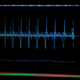
Here is an alternative circuit, where there are dividers and no reference filters, and this happens
 
pic1.png
pic2.png
pic3.png
the first graph is the initial data of instantaneous values (weight in grams on an empty platform), the second graph is a running average with averaging of 6 values, the third graph is also averaging of 15 values. In the graphs, to understand the time axis, 40 samples is one second, that is, the values on the horizontal axis must be divided by 40. Three types of noise are visible: high-frequency, which gives a scatter, medium frequency with a period of about once per second, small but noticeable amplitude, and low-frequency, which I described below as drift, is very large compared to the others in amplitude, but slow - tens of seconds and also with its lower harmonics.

weight measurement usually is rather low frequency. One usually does not need a data rate of more than 5 per second.
I agree with you, 5 measurements per second would be enough if they were stable, in my case the minimum is 20 measurements and they did not give such stability and I would like to try working with 45 measurements per second to be able to get more data, but then process them with a filter. By the way, you can see from the pictures that filtering makes some sense. By the way, if you measure with a change in excitation polarity, it turns out that the frequency of measurements will drop by another factor of two, since the end result is considered to be a pair of measurements.
In post#16 you talk about frequencies in the kHz. It is at least two (or three) magnitudes above what you need for a weigh scale.
Maybe you did chose an inappropriate IC at all. There are dedicated weigh scale ADCs (data acquisition systems).
In post #16, I tried to tell you what filters are available on the channels for measuring and supplying the reference voltage to the ADC, as well as what filters are on the device with the readings of which I am comparing my board.
This may be distracting, but I think it is also important information for those who may say that the choice is not correct, the cutoff frequencies are too high and need to be reduced. Although the device being compared, as already said, works with these values of filter cutoff frequencies.

Now you think that RS485 is too slow .. I can´t see why. RS485 bandwidth should easily go up to 1MBaud .. which should be suffiicient for way above 25kSamples/s.
In the previous posts I don´t see where RS485 is involved at all. So this new information just confuses me.
Also "MODBUS" is new information.
(Regarding MODBUS it depends what are the other connected devices on the MODBUS, other device´s data rates, baud rate options)

I also did not find the "data logger" information in the previous posts. If you post informtions piece-by-piece it´s not our fault to provide unsuitable recommendations.

Also "PC program" and "wrting on your own" ... is just another topic. I con only recommend: draw a signal flow sketch and solve the issues one by one form source to destination. Mixing all together is not very effective.
This was addressed to D.A.(Tony)Stewart. The point of this is that I was losing data when transferring to a PC (the display on my board shows data in real time in one-dimensional form, a graph cannot be displayed on a seven-segment display, there is no other option on the board) and the density of the survey did not allow me to take it in real time ("real time" - I don't need this at work, but it happened during debugging), but I did it a little differently and received the data in a package, which I then transferred to a PC and processed in Excel to build a diagram.
You don’t have to pay much attention to the interfaces and protocols; they are not for the ADC, but for connecting the board and the PC.
Drift over time: Simple to analyze.
Drift can be "offset drift" which does not relate to the applied weight (zero wight).
or it can be signal related: like "gain drift".
simply: if zero weight is applied and the result drifts by 0g +/-10g then it is offset drift.
If is is not offset drift, but you see the +/-10g drift only when 20kg is applied, then it is signal related. (Gain drift, Ref drift ...)

+/-10g on a 20kg load is 0.1% or just 10 bits of reliable information. --> No need for a 16 bit or even 24 bit ADC.

Klaus
To be honest, I don’t quite understand, firstly, when I have zero weight, in fact we have at least the weight of the platform, and secondly, the sensor may not be very well made and has its own offset, which, like the weight of the platform, I compensated with a mathematical offset . It turns out that I have a non-zero value for measurement on the ADC. I see drift even with applied weight (not 20 kg, of course, but only 2 kg for tests, but still there is drift too). It can also be seen in pictures (graphs).
 
Last edited:
+/-10g on a 20kg load is 0.1% or just 10 bits of reliable information. --> No need for a 16 bit or even 24 bit ADC.

Thats just A/D not including its errors or the entire signal path. OP should do a
complete signal path error analysis.Probably a 12 bit or slightly better would
satisfy. But again OP analytically do the signal path error analysis would be advised.


Regards, Dana.
 
Hi,
I agree with you, 5 measurements per second would be enough if they were stable,
I know what you mean. But averaging is good for reducing high frequency noise. But in your case it´s low frequency. You may average 1000 samples and still you will see the low frequency drift.
You need to analyze where this drift comes from. This si the professional way.
For sure you can do trial and error .. but this is tinkering - you don´t need us for this way.
The problem is: You may find a good solution for one device with the trial and error method. But the same solution may not work for the next device.
So if you want to build 100 pieces you need to try around 100 times.

By the way, if you measure with a change in excitation polarity, it turns out that the frequency of measurements will drop by another factor of two, since the end result is considered to be a pair of measurements.
Can´t agree. A measurement is a measurement.

the cutoff frequencies are too high and need to be reduced.
Don´t need to re-invent the wheel. Nyquist is true.
If you want to process up to frequency X you need to sample with MORE than 2*X.
If you violate this, then you may see alias frequencies. The problem is that alias frequencies are now in the frequency band of your interest, thus you can´t filter tham out on the digital side.
--> the only meaningful solution is to use an appropriate anti_aliasing_filter.
For me - as a professional measurement equippent designer - the use of appropriate filters is mandatory.

An example: you sample with nominally 16kHz. (XTAL accuracy). Then maybe there is a printer nearby with nominally 64kHz SMPS switching frequency (RC accuracy).
Lets say the XTAL is pretty accurate, but the SMPS has a tolernace of +/-1%. i.e. +/-640Hz.
So the alias frequency is 0...640Hz. The 640Hz end is not the problem, but let´s say the SMPS freq is 64010 Hz.
Then the alias frequency is 10Hz .. and you need an averaging filter of 1600 samples to rectify it.
Now due to temperature drift the SMPS frequency drifts by a tiny of 0.03% towards 16005Hz --> alias frequency 5Hz and now you need average 3200 to rectify this.
How do you know which averaging size you need?

Solution: get rid of alias frequency, by using the proper analog filter. As said, there are weigh scale ICs doing this for you. Mainly digital, to ease the analog part.

"real time" - I don't need this at work,
Wrong. Every weigh scale measurement I´ve seen is a real time application.
Measurement values come in .. while results go out.
You may have some delay between measurement and output, still it is real time.
You may use filters, you may have a data rate reduction, still it is real time.
You may have 10.000 samples/s or you may have 1 sample per day .... still both can be real time.

To be honest, I don’t quite understand, firstly, when I have zero weight, in fact we have at least the weight of the platform, and secondly, the sensor may not be very well made and has its own offset, which, like the weight of the platform, I compensated with a mathematical offset . It turns out that I have a non-zero value for measurement on the ADC. I see drift even with applied weight (not 20 kg, of course, but only 2 kg for tests, but still there is drift too). It can also be seen in pictures (graphs).
It´s on you to apply any weigh to the sensor. But then you need to treat the result that way. And if you want us to give useful reponse .. it´s on you to give this information first.
We can not know otherwise.
So, nothing changed. If you want to differ between offset drift and gain drift you need to ensure the sensor is without external force. Maybe you need to remove the platform, maybe you need to remove the sensor. We don´t know what you need to do. We don´t know the situation.
And yes, there will be sensor offset, but it should be far from 100% sensor load. It should be close to zero. And the absolute zero value does not matter anyway - it´s the drift we are talking about.
If it drifts +/-10g around zero .. it is offset drift.
If it drifts +/-1g around zero and +/- 10g around 2kg and +/-100g around 20kg .. it is mainly signal_related drift / gain drift.

Klaus
 
Some ref material that may be of interest, attached.

Keep in mind averaging works best on uncorrelated noise. But most of
our embedded systems these days have a lot of correlated noise due'
to clock generated noise for various onboard peripherals and its cpu.


Regards, Dana.
 

Attachments

  • an118.pdf
    407.3 KB · Views: 35
  • slaa510.pdf
    1.1 MB · Views: 32
RS-485 can do >100 Mbps per meter with STP cable.
So one divides by length to determine approximate limit on the cable.
Of course hardware limitations are yours. Are you using 6 Samples / s?

Parasitic drift from thermocouple effects of dissimilar metals are explained here https://www.ti.com/lit/pdf/tidubl0 on page 12 as well as preventable thermal drift from protection.

This can be fixed if that exists in your layout for 10 g/20kg correction.
 
Last edited:
RS-485 can do >100 Mbps per meter with STP cable.
So one divides by length to determine approximate limit on the cable.
Of course hardware limitations are yours. Are you using 6 Samples / s?

Parasitic drift from thermocouple effects of dissimilar metals are explained here https://www.ti.com/lit/pdf/tidubl0 on page 12 as well as preventable thermal drift from protection.

This can be fixed if that exists in your layout for 10 g/20kg correction.
I did this project based on it, although apparently TI decided to confuse me a little :). There is quote from it about filtering: As a tradeoff, a differential mode 3-dB cutoff frequency of 689 Hz and a common mode 3-dB cutoff frequency of 14.5 kHz was chosen, which gives the absolute minimum of 25-dB damping at the delta-sigma modulator frequency of 256 kHz.
And there is Schematic - TIDA-00765, and the data there is different, after all, having found the calculation words, I am inclined to believe that the data on the filters on Schematic - TIDA-00765 is incorrect.
(For all) In total, believe the following data: a differential mode 3-dB cutoff frequency of 689 Hz and a common mode 3-dB cutoff frequency of 14.5 kHz was chosen.
How do you think this is a normal choice of frequencies?
Some ref material that may be of interest, attached.

Keep in mind averaging works best on uncorrelated noise. But most of
our embedded systems these days have a lot of correlated noise due'
to clock generated noise for various onboard peripherals and its cpu.


Regards, Dana.
Thanks, I don't think I've seen it yet
Hi,

I know what you mean. But averaging is good for reducing high frequency noise. But in your case it´s low frequency. You may average 1000 samples and still you will see the low frequency drift.
You need to analyze where this drift comes from. This si the professional way.
For sure you can do trial and error .. but this is tinkering - you don´t need us for this way.
The problem is: You may find a good solution for one device with the trial and error method. But the same solution may not work for the next device.
So if you want to build 100 pieces you need to try around 100 times.


Can´t agree. A measurement is a measurement.


Don´t need to re-invent the wheel. Nyquist is true.
If you want to process up to frequency X you need to sample with MORE than 2*X.
If you violate this, then you may see alias frequencies. The problem is that alias frequencies are now in the frequency band of your interest, thus you can´t filter tham out on the digital side.
--> the only meaningful solution is to use an appropriate anti_aliasing_filter.
For me - as a professional measurement equippent designer - the use of appropriate filters is mandatory.

An example: you sample with nominally 16kHz. (XTAL accuracy). Then maybe there is a printer nearby with nominally 64kHz SMPS switching frequency (RC accuracy).
Lets say the XTAL is pretty accurate, but the SMPS has a tolernace of +/-1%. i.e. +/-640Hz.
So the alias frequency is 0...640Hz. The 640Hz end is not the problem, but let´s say the SMPS freq is 64010 Hz.
Then the alias frequency is 10Hz .. and you need an averaging filter of 1600 samples to rectify it.
Now due to temperature drift the SMPS frequency drifts by a tiny of 0.03% towards 16005Hz --> alias frequency 5Hz and now you need average 3200 to rectify this.
How do you know which averaging size you need?

Solution: get rid of alias frequency, by using the proper analog filter. As said, there are weigh scale ICs doing this for you. Mainly digital, to ease the analog part.


Wrong. Every weigh scale measurement I´ve seen is a real time application.
Measurement values come in .. while results go out.
You may have some delay between measurement and output, still it is real time.
You may use filters, you may have a data rate reduction, still it is real time.
You may have 10.000 samples/s or you may have 1 sample per day .... still both can be real time.


It´s on you to apply any weigh to the sensor. But then you need to treat the result that way. And if you want us to give useful reponse .. it´s on you to give this information first.
We can not know otherwise.
So, nothing changed. If you want to differ between offset drift and gain drift you need to ensure the sensor is without external force. Maybe you need to remove the platform, maybe you need to remove the sensor. We don´t know what you need to do. We don´t know the situation.
And yes, there will be sensor offset, but it should be far from 100% sensor load. It should be close to zero. And the absolute zero value does not matter anyway - it´s the drift we are talking about.
If it drifts +/-10g around zero .. it is offset drift.
If it drifts +/-1g around zero and +/- 10g around 2kg and +/-100g around 20kg .. it is mainly signal_related drift / gain drift.

Klaus
I seem to have decided on the filters (by cutoff frequencies): for a differential mode 3-dB cutoff frequency of 689 Hz and a common mode 3-dB cutoff frequency of 14.5 kHz was chosen.
If I understand correctly, it should help me reduce possible aliasing noise, that is, it will also work as an antialiasing filter. I just don’t quite understand how effective it is. How many decibels of attenuation should the filter have at the ADC sampling frequency Fmod/2? As I understand it, mine attenuates 20 dB per decade, I read about the requirement of 72 dB, mine certainly falls short at a frequency of 256 kHz/2.
By the way, if the sampling frequency is doubled (turbo mode), the noise only becomes more noticeable (although I expected a greater effect due to the greater attenuation of interference by filters at high sampling frequencies.), I think I already wrote this, although according to the documentation the indicators should not differ (the effective resolution and the number of bits without noise are identical for normal mode 256 kHz and 45 samples per second, and for turbo mode 512 kHz and 40 samples per second), in fact I chose the normal mode 256 kHz as a mode with less noticeable noise (with the same filtering and data processing methods, of course).
Regarding the definition of the type of drift, I now understand, well, it seems that the strength of the drift does not depend on the magnitude of the signal.

I want to thank everyone very much for trying to help me.
 
I put on a protective cable screen and twisted the wires from the sensor. As I already wrote, I bought it cheaply on Aliexpress, the sensor “out of the box” turned out to be completely unprepared for work. Once placed in a protective cable shield, the drift changed the picture significantly.
pic1.pngpic2.pngpic3.png
I didn’t think that conductors about 10-15 centimeters long could pick up so much interference.
 
Hi,

Drift vs noise. (just my personal opinion)
While both may have similar sources and similar effects on the output...in discussions they usually differ by the frequency.
* Drift is a low frequecny movement. Maybe caused by power supply fluctuations, thermal drift, aging ...
* Noise is the higher frequency error. Maybe caused by sharp edges of nearby signals, noise caused by the movement of the electrons.
There is no clear border between both. Some may sa high frequency is above 100MHz.
But when analyzing a ADC output with a sampling rate of 16kHz, then the upper frequency we can see is 8kHz. So the border shifts from application to application.

Alias frequency may contribute to both. Low frequency and high frequency.

Thus when I see the three pictures above: I see no improvement in drift, but I see improvement in noise.

Thus my opinion to your measurement problem is the same as mentioned in post#23: You need to focus on the low frequency problems.

Klaus
 
We can reduce this another -60 to -100 dB if you want. What do you need?
I suggest STP wire with shield to Agnd and RF cap to PE gnd. with copper gauze shield around board. It may be picking up grid noise mostly .

Then check noise. If still there, connect system to PE gnd by braid with DC or film cap.

Check noise again.

Reduce input noise BW in software as low as possible.

Check noise again.

I would check for SMPS noise getting in from somewhere !!

Then add 10 Hz 2nd to 4th order Op Amp Chebychev filter by adding small circuit. -75 dB @ 50 Hz (4th Order)
1705551991138.png


Scale R x100 C/100
Grid E-field noise can be 50 V/m but I think you have SMPS noise. Your fingers also make good antenna or gnd depending where they are.

For internal 1st order LPF to get what you need, you might need 64x to 128 x BW sampling rate. ( 20 dB/decade or -6dB/octave))
 
Last edited:
We can reduce this another -60 to -100 dB if you want. What do you need?
I suggest STP wire with shield to Agnd and RF cap to PE gnd. with copper gauze shield around board. It may be picking up grid noise mostly .

Then check noise. If still there, connect system to PE gnd by braid with DC or film cap.

Check noise again.

Reduce input noise BW in software as low as possible.

Check noise again.

I would check for SMPS noise getting in from somewhere !!

Then add 10 Hz 2nd to 4th order Op Amp Chebychev filter by adding small circuit. -75 dB @ 50 Hz (4th Order)
View attachment 188008

Scale R x100 C/100
Grid E-field noise can be 50 V/m but I think you have SMPS noise. Your fingers also make good antenna or gnd depending where they are.

For internal 1st order LPF to get what you need, you might need 64x to 128 x BW sampling rate. ( 20 dB/decade or -6dB/octave))
I've tried several tests. The first was to work with grounding, the manipulation does not have much effect now, because yesterday I attached the cable shield from another cable to this one (changing the cable itself is problematic, I twisted the existing one and placed it inside the shield, secured it with heat shrink). Considering that the cable shield is now connected through a 47 Ohm current-limiting resistor to the AGND polygon, the AGND polygon is connected through a thin section to the DGND polygon. I tried to connect grounding everywhere, but I didn’t see any significant difference. I think that the common-mode interference goes away through SMD capacitors.
I did the second test with a signal generator, applying millivolts to the input, I got an even greater scatter of readings (jitter), then short-circuiting the measuring circuit of the board (disconnecting the bridge wires from the board) I see the measurements still “dance” in approximately the same quantities as with the bridge . That is, the sensor itself and the conductors do not make noise.
Then I looked with an oscilloscope (although I don’t have a super accurate one, but I still wanted to look) with a 1:10 probe, I compared the 5V excitation power supplied from the DC/DC converter with a laboratory power supply (yes, I probably should have installed a separate DC/DC to 7V and then, using LDO, lower and stabilize to 5V, and use separately for excitation, without using these 5V anywhere else except AVDD of ADC, but I wanted to save some money, because I've also seen the same simple circuit in working device). The DC/DC noise, of course, turned out to be higher, but I cannot evaluate it due to lack of experience. The second measurement was made with a 1:1 probe. Photo attached. There you can see where the noise is less and where the signal is smooth - this is a couple of photos from a laboratory power supply.
20231219173644.png20231219173538.png20231219174359.png20231219174503.png
1-DC/DC probe 1:10, 2-laboratory power supply probe 1:10, 3-DC/DC probe 1:1
, 4-laboratory power supply probe 1:1
Judging by the pictures, there is noise, although according to the readings 20 mV, it doesn’t seem to be much, but perhaps it is enough to cause emissions to appear in the measurements.
In general, of course, visually, based on my experiments, what I got can be said to be enough, but for the sake of experience, I want to delve further (but more in my head, in my thoughts) further into issues of combating noise, but probably already on the next board. But with great pleasure I read suggestions and ideas and thoughts in general on this matter.
 
Last edited:
but I cannot evaluate it due to lack of experience.

If I´m not mistaken we did not see
* your schematic (all that is involved in the measurement)
* your PCB layout
* your wiring / shileding ... and the different test setups you made.

Textual descriptions simply saying are not suitable to descripe every single informations.
Screen shots, complete schematics, photos ... show the things how they really are.
And they show details that you (with this lack of experieince) simply do not recognize .. to generate an issue. And I don´t meant this to offend you, it´s just a matter of fact.

So if you want us to help you ... I recommend to provide these informations, so we are able to validate the full circuit.
Please reduce the file size of the photos to maybe 100kBytes each so that even members with low internet bandwidth are able to download them.

Klaus
 
You are referring to TIDA-00765 but also mentioned modifications. As KlausST, I'd expect a schematic of your actual design.

TIDA-00765 is using AC excitation. Your drift measurement are not using this technique?
 
You are referring to TIDA-00765 but also mentioned modifications. As KlausST, I'd expect a schematic of your actual design.

TIDA-00765 is using AC excitation. Your drift measurement are not using this technique?
My board allows the use of AC excitation, but at the moment I am trying to reduce noise with DC excitation (I don’t change the polarity using the keys), since AC excitation itself is used for slightly different purposes (fighting with parasitic thermocouples and other unipolar/unidirectional biases). At the moment I think that AC stimulation will not help much in current problem. Although I tried and looked, the scatter is also felt.
 
Hi,

since AC excitation itself is used for slightly different purposes (fighting with parasitic thermocouples and other unipolar/unidirectional biases)
Just to confirm:
I tried several times that exactly the low frequency drift is the biggest problem. Like thermocouple effects.
The higher frequency noise is rather simple to solve.

Klaus
 
How does noise + drift measurement with shorted ADC input compare to ADC spec?
I didn’t understand the question: did I draw the wrong conclusion based on the test with a short-circuited ADC input or, on the contrary, should I do such a test?
If anything, I did a test with a shorted input, I didn’t make a list of sample values, but I saw on the display that the low-order digit fluctuated with the same range as with the bridge connected.
 
Last edited:
When doing noise testing consider doing it with scope set on infinite persistence, that way
over time, say a few minutes, you will capture peak to peak noise. Allows you to find particular
problems, ones you cannot see easily, w/o "integrating storage" capability. When you do this
trigger on edge, a few mV should suffice. Additionally color grading if your scope has it will
add deeper insight into noise sources/origin.


Using CDS ( in this case specific micro but general principles apply)


and google "correlated double sampling ieee pdf"


Regards, Dana.
 
Last edited:
I didn’t understand the question: did I draw the wrong conclusion based on the test with a short-circuited ADC input or, on the contrary, should I do such a test?
If anything, I did a test with a shorted input, I didn’t make a list of sample values, but I saw on the display that the low-order digit fluctuated with the same range as with the bridge connected.
we don´t know the exact test conditions nor the exact results. (Test conditions also include PCB layout and power supply and so on...)
Thus we are unable to validate the test.

A fluctuating low order digit tells nothing, because an ADC is expected to fluctuate on the LSB .. or LSByte or LSDigit.
If you want to validate it you need to set up a useful test condition and do the tests properly. Best if you use the same test conditions as they used in the datsheet.
After the test you need to compare your test results with the datsheet specifications. I see no other method to validate whther your circuit operates properly or not.

I don´t want to annoy you by asking for the same again and again. And I don´t see any progress. Thus I leave it on you how to go on ... and I will come back when there is useful information as requested above.

Klaus
 
I've tried several tests. The first was to work with grounding, the manipulation does not have much effect now, because yesterday I attached the cable shield from another cable to this one (changing the cable itself is problematic, I twisted the existing one and placed it inside the shield, secured it with heat shrink). Considering that the cable shield is now connected through a 47 Ohm current-limiting resistor to the AGND polygon, the AGND polygon is connected through a thin section to the DGND polygon. I tried to connect grounding everywhere, but I didn’t see any significant difference. I think that the common-mode interference goes away through SMD capacitors.
I did the second test with a signal generator, applying millivolts to the input, I got an even greater scatter of readings (jitter), then short-circuiting the measuring circuit of the board (disconnecting the bridge wires from the board) I see the measurements still “dance” in approximately the same quantities as with the bridge . That is, the sensor itself and the conductors do not make noise.
Then I looked with an oscilloscope (although I don’t have a super accurate one, but I still wanted to look) with a 1:10 probe, I compared the 5V excitation power supplied from the DC/DC converter with a laboratory power supply (yes, I probably should have installed a separate DC/DC to 7V and then, using LDO, lower and stabilize to 5V, and use separately for excitation, without using these 5V anywhere else except AVDD of ADC, but I wanted to save some money, because I've also seen the same simple circuit in working device). The DC/DC noise, of course, turned out to be higher, but I cannot evaluate it due to lack of experience. The second measurement was made with a 1:1 probe. Photo attached. There you can see where the noise is less and where the signal is smooth - this is a couple of photos from a laboratory power supply.
View attachment 188010View attachment 188009View attachment 188011View attachment 188012
1-DC/DC probe 1:10, 2-laboratory power supply probe 1:10, 3-DC/DC probe 1:1
, 4-laboratory power supply probe 1:1
Judging by the pictures, there is noise, although according to the readings 20 mV, it doesn’t seem to be much, but perhaps it is enough to cause emissions to appear in the measurements.
In general, of course, visually, based on my experiments, what I got can be said to be enough, but for the sake of experience, I want to delve further (but more in my head, in my thoughts) further into issues of combating noise, but probably already on the next board. But with great pleasure I read suggestions and ideas and thoughts in general on this matter.
I like your scope, and efforts to isolate this problem.

Perhaps you just need some experience on how to make better signal captures to isolate the problem.

1:1 probes are useless >10 MHz unless terminated with 50 Ohms in DSO or on BNC "T" adapter with 50R inserted and very short wires& traces between source. and coax.

10:1 probes are useful to 200+ MHz but only if calibrated and coil spring adapters for scope probe with tip & gnd. removed you may choose to filter DSO with 20 MHz filter enabled hoping that it is just a measurement error. (the ground path inductance or ESL is on the order of < 1 nH/mm which resonates with probe coax capacitance ~70 pF/m on the ground side creating a high Q resonance > 20 MHz or gain of impulse noise in that band above 20MHz. )

What is the scaling factor from noise on DSO lowest noise for same on your ADC in terms of Vpp and BW.


I suspect some common mode point is getting converted into this differential noise somewhere either by conduction or radiation. (induction or stray capacitance but less likely with bridge signal shorted at source)

You may keep injecting noise into supply or ground or cable shield or try to detect the fundamental frequency of the noise on DSO with filtering.

For H field emissions use a fancy Rogowski coil probe or with some luck any 10:1 probe and coil or loop of wire with gnd clip to tip.
For E field noise emissions , use 10:1 probe tip to floating wire or foil and use stray capacitance to sniff for noise.
or use your finger and probe while suppressing grid noise with probe shorted to choke.
Probe loops come in various sizes.

For future reference, if you had a spectrum Analyzer they are even more sensitive to this using a DSO probe as an antenna to find the source of the conducted noise.

For what its worth all SMPS conduct some common mode noise via the transformer coupling capacitance and since the load is unbalanced compared to ground path, it gets converted into some amount of conducted differential noise. When your ADC is very sensitive or unbalanced over the measurement bandwidth, , unbalance anywhere in the measurement system can be degrade CMRR, even if it is a floating power supply. Thisis why CM chokes or Baluns are used with XY caps on inputs and ferrite and NPO caps used on DC outputs.

Remember ground by definition means 0 Volts but your tolerance to 0V will vary. It's just a reference point whether it is PE gnd or a floating ground or Agnd or Dgnd. This means the currents shared on these points may affect the voltage at gnd if another node is used.

I would start with 5V and expect to get a flat line AC coupled to coax into 50 Ohms on 1mV/div or lowest scale, then repeat on LDO then compare grounds.
 
Last edited:
Some ref material :

Keysight cutoff for passive probes ~ 600 Mhz (but then they counter that in other docs), as always
application dependent)


As one can see there strong application and associated application considerations
in wideband and low level signal observation, passive versus active probes.


Regards, Dana.
 

Attachments

  • 8 Tips for Better Scope Probings.pdf
    1.9 MB · Views: 32

LaTeX Commands Quick-Menu:

Similar threads

Part and Inventory Search

Welcome to EDABoard.com

Sponsor

Back
Top