Continue to Site

Welcome to EDAboard.com

Welcome to our site! EDAboard.com is an international Electronics Discussion Forum focused on EDA software, circuits, schematics, books, theory, papers, asic, pld, 8051, DSP, Network, RF, Analog Design, PCB, Service Manuals... and a whole lot more! To participate you need to register. Registration is free. Click here to register now.

Sample and Hold IC LF398

Status
Not open for further replies.

syee10

Member level 3
Joined
Apr 2, 2010
Messages
63
Helped
1
Reputation
2
Reaction score
0
Trophy points
1,286
Location
Malaysia
Activity points
1,758
Hi,

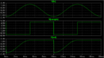
Anyone here can tell me how to connect a Sample and Hold IC LF398 in practical so that i can get a V(out) waveform as shown in the attached file? The V(in) and V(sample) is shown in the attached file also. Please provide me a simple schematic diagram if possible. The datasheet can be found in the following links:

LF398 pdf, LF398 description, LF398 datasheets, LF398 view ::: ALLDATASHEET :::
 

Attachments

  • SH4.png
    SH4.png
    15.2 KB · Views: 229

You need to invert your sample waveform. The LF398 "holds" when the sample input is low. You want it to hold when your logic signal is high.

Keith.
 

keith,

I think the sample waveform there should be correct. It shows the sample waveform and not the holding waveform. In fact i need to know how to connect the LF398 IC in order for me to get the output waveform. Can you help me? Thanks
 

Look at the proper version of the **broken link removed** - first diagram on page 1.

Keith.

---------- Post added at 11:22 ---------- Previous post was at 11:18 ----------

I think you are misinterpreting the word "sample". In your diagram it really means "hold". In the LF398 datasheet "sample" really means "track".

Keith.
 

keith,

I already try the circuit as what you shown me. But i dun know why i cant get the output correctly. If that is the correct circuit diagram i think i will try it again.
 

As I said, you must invert your "sample" logic signal.

Keith.

---------- Post added at 11:25 ---------- Previous post was at 11:23 ----------

By the way, where is that waveform from? It looks like an LTSpice simulation.

Keith.
 

keith,

Ok i understand what you mean. I will try this out in the lab again and lets see how. Thanks for your help =)
 

keith,

Can you explain to me what is the Logic Input Configuration in page 5 and page 6 in the datasheet talking about?
 

Ah right. It seems the "logic reference" pin 7 and "logic input" pin 8 are partly interchangeable and allow for setting the trigger threshold and also inverting the sample/hold logic. The first diagram on page 5 shows the normal operation. The next diagram allows you to reverse the logic, but you need to supply 2.8V to pin 8 to get a 1.4V threshold on pin 7.

On page 6 the first diagram shows an increased threshold voltage. The next shows an increased threshold but with inverted logic. The next two are similar different thresholds and showing the non-inverted and inverted logic.

So, you should be able to get your circuit to work without needing an external inverter. You just need to choose whether to use pin 7 or 8 for the control input and then set the voltage on the other pin according to the diagrams.

Keith.
 

keith,

Thanks for your explanation. I will try to make my circuit working tomorrow.
 

Status
Not open for further replies.

Similar threads

Part and Inventory Search

Welcome to EDABoard.com

Sponsor

Back
Top