Continue to Site

Welcome to EDAboard.com

Welcome to our site! EDAboard.com is an international Electronics Discussion Forum focused on EDA software, circuits, schematics, books, theory, papers, asic, pld, 8051, DSP, Network, RF, Analog Design, PCB, Service Manuals... and a whole lot more! To participate you need to register. Registration is free. Click here to register now.

S2-LP XTAL Design

Status
Not open for further replies.

leomecma

Full Member level 5
Joined
Jun 17, 2005
Messages
244
Helped
14
Reputation
28
Reaction score
1
Trophy points
1,298
Location
Brasil
Activity points
3,933
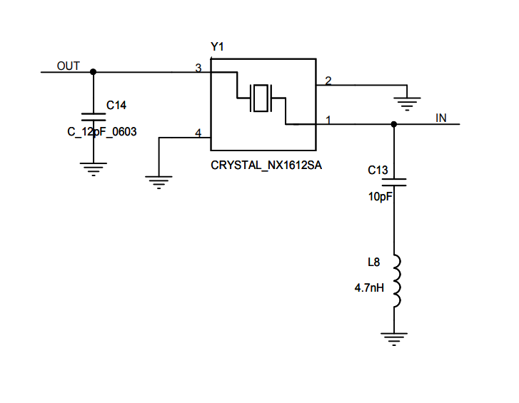
The ST Nucleo board X-NUCLEO-S2868A2 - Sub-1 GHz 868 MHz RF expansion board https://www.st.com/resource/en/data_brief/x-nucleo-s2868a2.pdf, use the XTAL configuration bellow
1643890198297.png


Someone know the reason of the inductor at input? Is this some kind of RF filter to 868MHz?


The same circuit is shown in an S2-LP application note, but without any explanation. https://www.st.com/resource/en/appl...r-the-s2lp-transceiver-stmicroelectronics.pdf

I can just guess that it's an absorption circuit to prevent radiated RF entering the crystal oscillator.
I suppose too, I think the values must be at resonance to be a short circuit at oscillator input for RF frequency. XL value is much less than XC at 50 MHz crystal frequency to disturb its operation.
 

The rejected frequency of C13, L8, is 734.1MHz, which doesn't tell much about the reason of the circuit.
Maybe I missed something, but myself I don't see this notch filter in any of the circuits from ST datasheet or AN, other than this X-NUCLEO module.
 

The circuit is also shown on page 14 in the AN linked in post #2, inductor value is however unspecified "TBD".
 

Status
Not open for further replies.

Similar threads

Part and Inventory Search

Welcome to EDABoard.com

Sponsor

Back
Top