Continue to Site

Welcome to EDAboard.com

Welcome to our site! EDAboard.com is an international Electronics Discussion Forum focused on EDA software, circuits, schematics, books, theory, papers, asic, pld, 8051, DSP, Network, RF, Analog Design, PCB, Service Manuals... and a whole lot more! To participate you need to register. Registration is free. Click here to register now.

Routing to Vias

jimmykk

Full Member level 3
Joined
Oct 2, 2014
Messages
158
Helped
0
Reputation
0
Reaction score
1
Trophy points
1,298
Activity points
2,863
Hi
I have a Power connection passing from Diode to Surrounding Vias and into underlying Power Plane.
Current through this Power Connection would be maximum 2-3A.
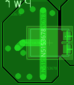
1693399472590.png

Just wondering if routing the copper lines directly from Diode to only 3 vias is a good practice? There is Copper plane surrounding all the 10 vias.
Or should it be left like this below:
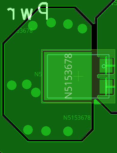
1693399572114.png

Vias have 0.5mm diameter.
 
i don’t understand. the top layout shows a trace running across the pad connecting to the copper plane. the bottom layout shows no connection. Are we to assume the diode pad and copper are two different layers? If so, why is the copper missing from under the pad? if they’re the same layer, why not connect pad directly to copper ( with thermal relief)?
 
Hi,

It´s not clear to me either.
and don´t forget: the diode may need some heat spreading .. also usually done using vias and copper planes.

Klaus
 
Sorry the below picture should actually be like this:

1693467806664.png


When i deleted the traces to vias, it somehow was not updated.
 
Hi,

did you read Barry´s post about the layers?

It´s all in green, so do we have to guess it´s all in one layer?

A bit more information .. will result in better answers.

Klaus
 
To improve heat disspation, you'll typically avoid thermals with SMD power components. Reflow solder will heat the whole PCB and in so far doesn't necessarily require thermals. Hand solder and rework are of course easier with thermals, at the cost of limited component heat dissipation.

Datasheet current ratings are usually expecting a copper area directly connected to the component.
 
Yes everything green means its on one(Top) layer. Have not shown any underlying layers.
So, basically the question was whether it is good practice to connect Diode Copper pad to surrounding Copper as shown in the picture i posted today
OR
the first picture from yesterday is better choice where Diode Copper Pad is connected directly to Vias in the surrounding Copper.
 
If everything green is in one layer, then the top picture of post#1 the traces just act as "wider" thermals in the tiny space between PAD and copper area. Besides the thermal width there is no difference to the picture in post#4.
All the rest where the traces overlay the other area is useless, since it is already copper. ... and obviously will not increase copper thickness at the overlayed area.

Klaus
 
You need to determine how much heat you need to dissipate, and how easily you want to be able to unsolder that part. Youre just not providing any information.
 

LaTeX Commands Quick-Menu:

Similar threads

Part and Inventory Search

Welcome to EDABoard.com

Sponsor

Back
Top