Continue to Site

Welcome to EDAboard.com

Welcome to our site! EDAboard.com is an international Electronics Discussion Forum focused on EDA software, circuits, schematics, books, theory, papers, asic, pld, 8051, DSP, Network, RF, Analog Design, PCB, Service Manuals... and a whole lot more! To participate you need to register. Registration is free. Click here to register now.

Ring oscillator design

Status
Not open for further replies.

digital design

Junior Member level 2
Joined
Oct 27, 2012
Messages
20
Helped
0
Reputation
0
Reaction score
0
Trophy points
1,281
Visit site
Activity points
1,446
Hi
I need to design a ring oscillator on FPGA. I create it by a chain of inverters and one AND gate for reset oscillation. There is no problem in simulation but when I program FPGA, it doesn't work and I don't know why!!
I use IGLOO Actel FPGA.
Please guide me.
thanks
 

It doesn't work because ring oscillators are touchy little creatures.

Chain of inverters. Okay, good start. How many inverters did you use? Suppose you used 5 or so, what you want to do is split up that chain in two parts and then put a placement constraint on them. You put 2 inverters over there, and the other 3 inverters waaaay over there on the die. That should give you 1) long routing delay 2) yesyes no doubt a lower frequency than the awesome 1 GHz you were trying to get and 3) a good chance of it actually working.

Oh and you want to put a FF as a divide by 2 stage after the output. Just because you can. And because it helps in getting a roughly 50% duty cycle.

Hope that helps. :)
 
  • Like
Reactions: Godup

    Godup

    Points: 2
    Helpful Answer Positive Rating
Also, make sure your synthesis tool is not eliminating those redundant inverters. Logically, 1 inverter is the same as 99 inverters and unless you force the tool to leave those inverters alone, it will optimize them away.

But (IMO) don't use a ring oscillator, you're just asking for trouble. If you can afford an FPGA in your design, you can afford an external oscillator.
 
  • Like
Reactions: Godup

    Godup

    Points: 2
    Helpful Answer Positive Rating
Thanks for your guidance. I don't know how I should split up the chain and force it to implement two inverter chains far apart!
I don't know how I should set constraint!! I guest Synplify tool optimize circuit and remove all buffers and inverters! I should force it to keep all of them but I don't know how!
Can you help me in this way?

- - - Updated - - -

I want to use Flash*Freeze mode of IGLOO kit. When an IGLOO device is in Flash*Freeze mode, none of the input signals (external clock) are seen by the internal logic. so I must create a ring oscillator in FPGA that is the internal clock source to the design.
I follow attached documentation step to step. About ring oscillator there is no problem in simulation but I have some problems on board. Ring oscillator didn't work on board. there are 4 step in section ring oscillator of this documentation. I can't set constraint of step 3.
 

Attachments

  • FlashFreeze_Ctrl_using_IOSC_AN.pdf
    281.5 KB · Views: 215

I am not familiar with Actel parts or that kit you're using, etc., but in Synplify you can use the "preserve" attribute to keep elements from being optimized out.
 
I would assume you have read the application note on the MicroSemi website about that topic? It points you in the good direction.
 

It doesn't work because ring oscillators are touchy little creatures.

Chain of inverters. Okay, good start. How many inverters did you use? Suppose you used 5 or so, what you want to do is split up that chain in two parts and then put a placement constraint on them. You put 2 inverters over there, and the other 3 inverters waaaay over there on the die. That should give you 1) long routing delay 2) yesyes no doubt a lower frequency than the awesome 1 GHz you were trying to get and 3) a good chance of it actually working.
Oh and you want to put a FF as a divide by 2 stage after the output. Just because you can. And because it helps in getting a roughly 50% duty cycle.

Hope that helps. :)


Thanks for the break down but pls throw more light (enlighten) on using FF as a clock divider. How is it done? Kindly give a sketch of design and attach to your comment. Am also experiencing a similar challenge.

- - - Updated - - -

Also, make sure your synthesis tool is not eliminating those redundant inverters. Logically, 1 inverter is the same as 99 inverters and unless you force the tool to leave those inverters alone, it will optimize them away.

But (IMO) don't use a ring oscillator, you're just asking for trouble. If you can afford an FPGA in your design, you can afford an external oscillator.

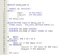
Am also experiencing a similar challenge, but unfortunately i would have to use a ring oscillator because am designing the chip to respond to temperature changes. How do i get to know if the tool (QUARTUS II) had optimized the ring oscillator and where in the tool can i force it to stop optimizing the design? Attached is a snapshot of my code (VHDL) and the netlist viewer of the design. Thank you
 

Attachments

  • couple RTL.JPG
    couple RTL.JPG
    124.6 KB · Views: 167
  • Couple Tech Map viewer.JPG
    Couple Tech Map viewer.JPG
    196.4 KB · Views: 183
  • Ring Osc.JPG
    Ring Osc.JPG
    44.2 KB · Views: 160

Use the ring osc output as a clock, route clock to clock input of FF. Slap on an inverter and you're done.

Code:
reg divided_clk;

always @(posedge ring_osc_clk)
    divided_clk <= ~ divided_clk; // divided clock at half the frequency of ring_osc_clk
 
  • Like
Reactions: Godup

    Godup

    Points: 2
    Helpful Answer Positive Rating
Thanks for the quick one... but i like to know if that code is VHDL, i would prefer VHDL. Also what kind of FF? +++ Slap on an inverter what does it mean???
Use the ring osc output as a clock, route clock to clock input of FF. Slap on an inverter and you're done.

Code:
reg divided_clk;

always @(posedge ring_osc_clk)
    divided_clk <= ~ divided_clk; // divided clock at half the frequency of ring_osc_clk
 

The above code is for a FF, with the output connected to an inverter, and that output is going back to the FF input. As in toggle the flip-flop on each positive edge of the clock.
 
  • Like
Reactions: Godup

    Godup

    Points: 2
    Helpful Answer Positive Rating
Am also experiencing a similar challenge, but unfortunately i would have to use a ring oscillator because am designing the chip to respond to temperature changes. How do i get to know if the tool (QUARTUS II) had optimized the ring oscillator and where in the tool can i force it to stop optimizing the design? Attached is a snapshot of my code (VHDL) and the netlist viewer of the design. Thank you
You are doing it basically right with syn_keep attribute. To view the delay_line details, you just ned to double click the block. You can also look at the resource usage to know if the ring oscillator has been implemented.
 
  • Like
Reactions: Godup

    Godup

    Points: 2
    Helpful Answer Positive Rating
Thank you.. i got it now, i appreciate ur post. But do you know how to force a compiler from optimizing a design on the Quartus II software??? Or is there a Reserved word in VHDL that could do that?


Use the ring osc output as a clock, route clock to clock input of FF. Slap on an inverter and you're done.

Code:
reg divided_clk;

always @(posedge ring_osc_clk)
    divided_clk <= ~ divided_clk; // divided clock at half the frequency of ring_osc_clk
 

I'm not that familiar with Quartus. You'd have to read the constraints user guide for that sort of thing.
 
  • Like
Reactions: Godup

    Godup

    Points: 2
    Helpful Answer Positive Rating
Thank you.. i got it now, i appreciate ur post. But do you know how to force a compiler from optimizing a design on the Quartus II software??? Or is there a Reserved word in VHDL that could do that?
Thanks FVM, just answered that!

- - - Updated - - -

You are doing it basically right with syn_keep attribute. To view the delay_line details, you just ned to double click the block. You can also look at the resource usage to know if the ring oscillator has been implemented.

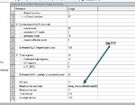
Thanks man... got those block starring at me... didn't know i needed to double click. Attached is what it looks like. Pls assess.
 

Attachments

  • Chain.JPG
    Chain.JPG
    17.3 KB · Views: 118
  • Resource usage.JPG
    Resource usage.JPG
    70.7 KB · Views: 128

Why are you now showing RTL instead of gate level view? RTL doesn't tell about logic removed during optimization.

You might be confused by the parallel 80 bit inverter, that's how things are compacted in RTL view.

The logic gate usage of the respective sub-entity is the most simple way to check if the inverter chain has been implemented.

Thanks, i got it now. Do u have any ideal as to forcing split on ring oscillator as mrflibble suggested? How is this constraint done in VHDL???
 

I don't see why we should split a ring oscillator.

Nevertheless you are free to prescribe an exact postion for each logic cell in assignment editor (presumed you understand the syntax).
 

What he meant to ask was "How do I constrain something to a particular location?" aka read the fine manual.
 

Nevertheless you are free to prescribe an exact postion for each logic cell in assignment editor (presumed you understand the syntax).

Not too sure about syntax now but my code is structural so created several objects of the ring oscillator attached together by SIGNAL lines. Then in assignment editor i found pins assigned... so where exactly can a do position fixing???

- - - Updated - - -

aka read the fine manual.
. is it a material (for the tool or device)??? do i have to download that or its in the tool already (where can i get it)???

- - - Updated - - -

I do hope u don't mean node assignment/location for logic placement.
 

Status
Not open for further replies.

Part and Inventory Search

Welcome to EDABoard.com

Sponsor

Back
Top