Continue to Site

Welcome to EDAboard.com

Welcome to our site! EDAboard.com is an international Electronics Discussion Forum focused on EDA software, circuits, schematics, books, theory, papers, asic, pld, 8051, DSP, Network, RF, Analog Design, PCB, Service Manuals... and a whole lot more! To participate you need to register. Registration is free. Click here to register now.

RF enabled power supply

Status
Not open for further replies.

muncle

Newbie
Joined
Dec 15, 2022
Messages
3
Helped
0
Reputation
0
Reaction score
0
Trophy points
1
Activity points
51
Hello all. I'm attempting to design an RF enabled battery powered design. I have a small AAAA powered pcb with a pic and a SI4467 XCVR communicating at 915MHz with another system. This part is designed and working with the help from SI4467 reference designs. However, per external requirements I need the circuit to only operate in the presence of a separate 868MHz signal (non latching). Rather than putting things in sleep/shutdown mode I need to disable the dc/dc converter because there are various other parts (pullups etc) that will drain the battery. I will need to use ANT-868-CHP-T chip antenna.

It was suggested elsewhere that I use the following circuit to generate an enable signal for the power supply...

Q05HJEF.png


SI AN768 suggests using the following matching circuit for the before mentioned chip antenna...
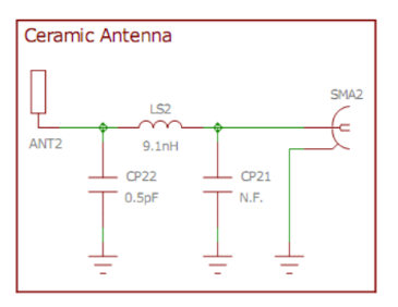
q0hC1gF.png


That all being said, RF is my weakness and I'm not sure what the thinking is behind the enable circuit (Aside from the high side switch). I've tried simulating all this in ltspice and it doesn't seem to work but I'm sure I am missing something.

fGszK9u.png


Attached is the .asc file for the simulation. In the simulation I'm alternating between switching in an 868MHz signal, no signal, and a 915MHz signal and would like to see the enable go high only in the presence of the 868MHz signal. I know I need some filtering but I'm not sure how to in conjunction with the suggested circuit.

Help!
 

Attachments

  • Draft1.zip
    1.3 KB · Views: 133

Your antenna link appears to list one for 868 MHz. My simulations indicate you can boost amplitude 2x or 3x by following with a bandpass filter made from an LC 2nd order.

It's a simple design easy to construct. This illustrates a principle although you can probably find a type with more components and a steeper rolloff curve.

LC 2nd order bandpass boosts 868 MHz AC.png
 

This seems to completely filter out the signal except for a small impulse when 868MHz turns on at 2ms.
1671209269144.png


1671209303717.png
 

Yes, now I see I also get a strong spike when the 868MHz source is shut off abruptly. I believe it's inductive kick. It creates false responses.

An alternate arrangement is to reverse the positions of L & C. That's a conventional second order filter.

As many as 5 cycles of the waveform must go through the system (10 nSec) as amplitude builds.
 

That's all dandy but my real goal is to drive the high side switch which is the real crux of the problem.
 

If you want a really tight detect-band, you might consider a cheap PLL and use its lock detect output. One for older low cell band is probably all the way price compressed. But those are needier than a simple envelope detect on a bandpass filter. And maybe -too- tight.

Looking at the old LM567 datasheet and app notes might give you ideas, despite it being Mhz rather than Ghz capable. At least it was simple enough to fit in an 8-pin DIP, and better transistors can be had. There could be a similarly-simple RF detector product, this is not really my forte either....
 
That's all dandy but my real goal is to drive the high side switch which is the real crux of the problem.

Your enable schematic (image #1) presupposes something crucial about the incoming signal...
Namely that it's strong enough to activate the transistor.

The waveform must make its way through a few components. These have the effect of attenuating the amplitude. Then it arrives at the bias terminal. By that time it must still be: a) sufficient voltage and b) sufficient current, to turn on the transistor.

Obviously in order to achieve this, the antenna needs to begin with generating a strong enough waveform.

Is this the case? The chip antenna is advertised as high-performance and high-efficiency. Maybe it really can do the job. I spot a CLC filter (image #2). Perhaps it's designed to apply a certain amount of gain, at 868 Mhz. (In similar manner as my post #2 intends even though I didn't test it with hardware).

Your own experiments with simulations and hardware is the path of progress toward reaching a solution.

You may find the first schematic is unusable in its present form. Your aim is to take full advantage of transistor gain, and sensitivity to a weak bias signal.
 

Status
Not open for further replies.

Part and Inventory Search

Welcome to EDABoard.com

Sponsor

Back
Top