coolsaurabhsonu
Junior Member level 1

- Joined
- Jan 10, 2011
- Messages
- 19
- Helped
- 0
- Reputation
- 0
- Reaction score
- 0
- Trophy points
- 1,281
- Activity points
- 1,413
Hi,
i am working on Voltage controlled delay line (VCDL) for Delay locked loop(DLL).
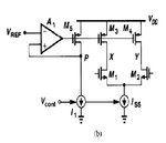
i started VCDL design using Replica Bias which is given in razavi book(Fig attached).
as mentioned in book, For VDD= 3.3V , i kept VREF = 2.1V , so that to have swing of 1.2V.
And kept both M3 and M4 in linear region. The problem i am facing is :
1. The MOS operation in Linear region is not acting as a linear resistor for complete swing.
2. Both charging and discharging of the output node is different (Vx, Vy).
i din't understood why this is happening.please help me to explain:
1.Why this charging and discharging rate are not same.
2.MOS operating in linear load (M5), is it sufficient to keep Vp = VREF.
3.How a symmetric load (concept by Maneatis paper) can solve this problem. how it acting as a linear load.
please help..........
