Continue to Site

Welcome to EDAboard.com

Welcome to our site! EDAboard.com is an international Electronics Discussion Forum focused on EDA software, circuits, schematics, books, theory, papers, asic, pld, 8051, DSP, Network, RF, Analog Design, PCB, Service Manuals... and a whole lot more! To participate you need to register. Registration is free. Click here to register now.

Reducing ringing in a DC/DC converter

Status
Not open for further replies.

mike buba

Member level 3
Member level 3
Joined
Nov 17, 2013
Messages
55
Helped
0
Reputation
0
Reaction score
1
Trophy points
1,288
Activity points
1,733
Hi. I am trying to reduce ringing. So far I have tried several things suggested here
1) Minimize DC-link inductance - I used aluminium plates to connect DC-link capacitors instead of cables​
2) I added a SiC Schottky diode in parallel with the IGBT body diode​
3) Increases RC Snubber circuit from 1uF to 1.5uF​
4) I have not yet increased gate resistance.​

I have recorded a few oscillograms around the IGBT chopper module to better understand the situation, but I cannot see the ringing in the voltage across IGBT. However, in this document (fig. 8, page 13.) y-axis is voltage and shows ringing.

In oscillograms I cannot see ringing in voltage, only in the current waveform coming into IGBT (?!).
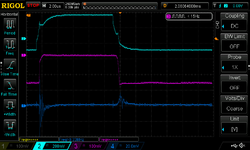
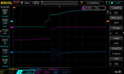
Ch2: PWM pulse gate-emitter
Ch3: Voltage across IGBT
Ch4: current coming into IGBT
Schematic (detail)
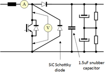
Model.png
Oscillograms: Full pulse
DS1Z_QuickPrint70.png
Turn-on detail
DS1Z_QuickPrint68.png
Measured ringing frequency approx. 8 MHz
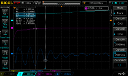
DS1Z_QuickPrint69.png

Is there anything else I can do? I do not feel changes 1) - 3) helped that much.
The last thing I can do is increase the gate drive resistance, but not sure if this will also make any significant difference; as there is currently no ringing in the voltage waveform.
 
Last edited:
Hi,
Minimize DC-link inductance - I used aluminium plates to connect DC-link capacitors instead of cables
This maybe decreases DC resistance, but does not necessarily reduce the inductance or impedance.

ringing usually issome kind of resonance problem with L and C.
So adding a diode, may add C and thus does not reduce ringing, ringing amplitude, ringing decay time. But it may reduce the ringing frequency.
To improve ringing decay time you need to decrease the stored energy in the ringing system or you need to improve than this energy is dissipated as heat. --> resistor. reduce Q. But adding capacitance and making traces more low resistance does not necessarily reduce ringing.

Thus I see
* the use of an RC snubber --> you need to adjust the R to disspate the energy at resonance frequency.
* or reduceing dV/dt as good approches.

****
But often the ringing isn´t that bad as it seems, because the test (scope with it´s probe and wiries) may increase ringing, or even show ringin that does not exist (ground bounce, echoing)
So be sure that the ringing you see really exists, otherwise you fight against a ghost.

Klaus
 
Hi Mike,
What diode is your using as a boost diode?. Due to it is a boost configuration, the critical component regarding ringing on the switching node is the boost diode. It must be a low trr diode or SiC ideally, otherwise, there will be a big ringing due to the recovery reverse current.
Byjuncal
 
What diode is your using as a boost diode?. Due to it is a boost configuration, the critical component regarding ringing on the switching node is the boost diode. It must be a low trr diode or SiC ideally, otherwise, there will be a big ringing due to the recovery reverse current.
It is a SKM100GAL12T4 IGBT module.
It does not say trr, but gives Qrr = 15.7 uC. As a comparison, SiC Schottky I am using to bypass the IGBT body diode is 125 nC.
I can use a second diode from the existing SiC diode and put it in parallel.
 

How are you measuring the IGBT current? What's the scale factor (for all three traces, actually)? Is ch3 supposed to be inverted?

The current trace in those scope captures doesn't look anything like one would expect for a boost converter, at least one that's passing significant power. Based on that, and the fact that the voltage waveforms don't have similar ringing, I'm guessing the current measurement isn't useful at all.
 

The first issue (to me) is, that probe tip capacitance and the
boost inductor and the supply bypass caps make a tank with
the IGBT across it. I've seen a 7pF probe really "enhance"
ringing on the VIN rail when applied to the SW node. May
want to determine whether the act of measuring is causing
what you measure.

Believe what you are seeing, for good reason, before you
try to hunt down and kill it. Otherwise it may be a long and
fruitless "snipe hunt".
 
I'm with mtwieg. Rather unlikely to see real current ringing with almost montonous voltage waveform.

What's current waveform scale factor, what kind of current probe are you using? What's the boost inverter load case?

Another thing. External parallel diode rarely improves switching behaviour of a poor internal diode.
 

yes, youre unlkely to short out the igbt diode with an external sic...as sic has higher vf, usually.
Yes byjuncal is right, its the boost diode you need to pay attention to.
Also, the waveforms dont make much sense for a heavily loaded booster, as above says.....there isnt much current at all....it just looks like the current tool isnt connected but its wires are near the converter, and picking up common mode noise from the converter.
 
Last edited:

yes, youre unlkely to short out the igbt diode with an external sic...as sic has higher vf, usually.
Yes byjuncal is right, its the boost diode you need to pay attention to.
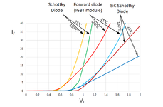
Yes. It seems that SiC Schottky across the IGBT body diode isn't doing much as SiC VF is bigger. For the forward diode, I will bypass it with SiC Schottky diode, i.e. leave IGBT module diode output pin unconnected.
I have plotted VF vs IF for the IGBT module diode, SiC Schottky diode I am using and one Schottky diode; and it seems even Schottky diode will not make much difference at my max. IF (5 A) and almost identical VF0.
Cmp.png

Also, the waveforms dont make much sense for a heavily loaded booster, as above says.....there isnt much current at all....it just looks like the current tool isnt connected but its wires are near the converter, and picking up common mode noise from the converter.
It is the Active PFC configuration, in open-loop for this example, so part of the period the current is zero. It is recorded at low current, low voltage.
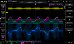
Open-loop (Ch3: Inductor current, Ch4: Grid line current)
DS1Z_QuickPrint46.png
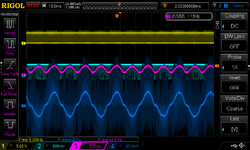
Closed-loop (Ch3: Inductor current, Ch4: Grid line current)
DS1Z_QuickPrint48.png
Ch3 is the filtered current probe (it has an RC filtering block before entering scope), and Ch4 is the unfiltered current probe.

Now I am trying to find out where that common-mode noise is coming from.
 

Now I am trying to find out where that common-mode noise is coming from.
...it willl just be in the ambience all around the circuit, due to the switching, the high dv/dt especially
 

Status
Not open for further replies.

Similar threads

Part and Inventory Search

Welcome to EDABoard.com

Sponsor

Back
Top