Continue to Site

Welcome to EDAboard.com

Welcome to our site! EDAboard.com is an international Electronics Discussion Forum focused on EDA software, circuits, schematics, books, theory, papers, asic, pld, 8051, DSP, Network, RF, Analog Design, PCB, Service Manuals... and a whole lot more! To participate you need to register. Registration is free. Click here to register now.

question : power mosfet turn ON waveforms

Status
Not open for further replies.

cmos_ajay

Full Member level 2
Joined
Jan 30, 2007
Messages
126
Helped
0
Reputation
0
Reaction score
0
Trophy points
1,296
Activity points
2,247
Hi,
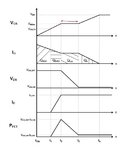
Attached is a waveform of a power MOSFET turn on procedure.
* I would like to know why the Cgs ( gate source capacitance) has a constant voltage across it during time interval T2 to T3 ?
* Why does Cgs 'not' charge during T2 to T3 ?
This is called as a Miller plateau region, but the text book explanation is not clear to me.
Can someone explain ??
 

Attachments

  • mosfet turn on.jpg
    mosfet turn on.jpg
    40.5 KB · Views: 69

Miller capacitance is another name for Cgd. Between T2 and T3, all gate current will go into Cgs. This happens under the assumption that the load is drawing a constant current, which is an almost realistic asumption in case of inverter circuits with output inductor.
 

Cgs swing comes from converting the depletion region to
inversion, now you "hook up" the area under the gate
(Cox) to the source via the channel. There is only so
much charge to be put, for a fixed Vgs, and it all happens
before to shortly above threshold.

Then the drain begins to swing, and that high drain
drain voltage across drain-gate capacitances is the
plateau charge. Vgate/RgateDrive = I = Cds*dV/dt,
generally the fixed gate drive creates a linear ramp
on the FET drain, and this is why low output impedance
gate drivers are needed for high frequency & efficiency.
 

Status
Not open for further replies.

Similar threads

Part and Inventory Search

Welcome to EDABoard.com

Sponsor

Back
Top