Continue to Site

Welcome to EDAboard.com

Welcome to our site! EDAboard.com is an international Electronics Discussion Forum focused on EDA software, circuits, schematics, books, theory, papers, asic, pld, 8051, DSP, Network, RF, Analog Design, PCB, Service Manuals... and a whole lot more! To participate you need to register. Registration is free. Click here to register now.

Question on package creation in Eagle.

Status
Not open for further replies.
Thanks again Keith.

1) How do you snap components into the grid you choose? I have to lock a lot of the components like potentiometers and connectors in particular position and I have to put the grid into 5mils in order to get to the mechanical specifications. I made a mistake of moving the other components, now they are in grid 5!!!. I want to layout the rest at grid 25 or 50, but it would not snap to grid. I search in help and no luck. Is there a command of snapping components into grid as soon as you pick in MOVE? OrCad will pick up the component and snap into the grid you set.

2) When you route trace, is there way to switch ends? Say if you route from point A to point B, right in the middle of routing from A to B, can I switch to point B and start routing towards A? This is a feature of OrCad that you route half way, then you switch to the other end and see how it two meet.

3) When I place the components on a net that go to many points, is there a command to minimize the connections to get the most straight forward path? This is a feature of OrCad that is very important.

Thanks

Alan
 
Last edited:
I have to do this from memory for now.

1. Hold CTRL when you pick it up to move resnaps to grid.

2. Not that I know of. I normally just drop it and pick it up again further along. I have a function key programmed for ROUTE so it is a quick procedure.

3. RATSNEST recalculates the paths (I think that is the name). There is usually an icon for it - a dot in a square of dots.

Keith
 
Hi Keith

I finished placing the components and I put the polygon on the top layer with net connect to GND. I accidentally click the Ratsnest and the copper pour on the top layer show up, how can I toggle to make it disappear and turn it on again?

Thanks

Alan
 
Last edited:

There is an option to select if 'ratsnest pours polygons' - under OPTIONS SET I think. Otherwise, quit and come back into the package.

Keith
 

There is an option to select if 'ratsnest pours polygons' - under OPTIONS SET I think. Otherwise, quit and come back into the package.

Keith

Thanks for the reply, I don't quite get it. I went to the Option, Set, pour Polygon, then I check and uncheck, nothing happened. I just cannot get rid of the copper fill. Any way to set a new layer for polygon at the top layer in the Display so I can turn it on and off?

Do you find the tuitorial and manual very hard if not impossible to understand? It seems like they try to explain in a top down, high ache form that define the way the software run RATHER than just explain the steps to get the job done. As I said, I had no issue learning other CAD software like OrCad, Microwave Office and Quartus for designing Altera FPGAs. Those are not simple programs if not more complex than Eagle. But all of them explain in a much simple manner that if you have a question, you type in search, it will just simply give you step by step on what to do. I find the Eagle absolutely frustrating to learn if not with your generous help. Even when you tell me to look you simple thing in search, I have problem follow the material. Case in point about the snap to grid, I still end up had to do some trial and error to find my way, then write it down in my own notes!!! I believe I am very good in self taught as I learn all the above programs myself, I just can't get this one!!!

I gone through quite a few Youtube video that really help, but I have not find the details that I have been asking you. They are more the introductions.

Thanks

Alan
 
Last edited:

You need to quit Eagle and go back in after checking the box. I am not sure if there is an 'unpour' command.

Often when making 2 layer board with ground plane I start off with a 4 layer with an inner layer for ground. Then I can route the ground and turn it off.

When I have finished I remove the inner layer and move the plane to the layer I want. There may be another way of doing it.

Keith


Ha Ha, I only have the trial version that can do 2 layers only. I am still try to justify whether I like it enough to pay for it. I just add a long comment into my last post.

Thanks

Alan
 

I cannot really comment on ways to learn Eagle because I have been using it so long. I found it easy to pick up and had been using Orcad prior to that. Earlier I had used Ultiboard & Boardmaker.

I found the official Eagle newsgroup useful when I was starting. No so much to ask questions but the answers were often already on there.

Keith
 

One other thought - I seem to remember you can get time limited version through Element14 (Standard version I think). That might be worth checking.

Keith
 

You need to quit Eagle and go back in after checking the box. I am not sure if there is an 'unpour' command.

Often when making 2 layer board with ground plane I start off with a 4 layer with an inner layer for ground. Then I can route the ground and turn it off.

When I have finished I remove the inner layer and move the plane to the layer I want. There may be another way of doing it.

Keith

Wow, that is inconvenient!!

Also I have more question now that I am doing routing.

1) In OrCad, when you route, you try a path, and if you don't like it, all you have to do is hitting "G" key. Every time you hit G, the very last segment you routed will be unrouted. You hit G again, the second last segment routed will be unroute. So you basically can back track your routing. Is there any function like this in Eagle? So far, using the unroute command is very inconvenient because you have to stop, click the command, then click each trace. The worst of it all, the net after unroute stay the same as the original trace.

2) Is there a command to bring the bottom layer up for display. I can't get rid of the copper polygon at the top layer, then I can't see the trace I routed in the bottom layer!!! I have to get out and come back?

3) I have problem selecting the object to move. Does Eagle have command that make the selection to limit to either components, routing traces, polygon etc. So I can choose specific object to move and not accidentally activate the wrong object.

Do you have problem in the display when you route and un-route? When I was doing the routing, the display went funny all the time and you can see image overlap. I had to zoom out and in to clear it. It felt like a software bug.
 

Personally I don't find moving the layers a problem. It old takes a few seconds (define the inner layer as a power plane) and gets rid of the power and ground without it showing up.

1. UNDO/REDO are usually programmed to the F9/F10 keys. If not, you can set them.

2. type

RIPUP @;

on the command line (or program a function key to do that).

3. Selection of components is based on the origin (usually a visible cross). Only origins that are visible can be selected. If two or more components or tracks are close then it will highlight one and you can cycles on to the others until you see the correct one. Zooming in tends to minimise such problems.

I don't have any display issues. It could be a problem with your graphics driver although I doubt Eagle uses anything fancy there. I am still using 5.11 so it could be a "new" problem.

Keith
 
Thanks Keith

I have complete the routing, set DRC and Check DRC already. I have manage to set copper polygon to pad clearance and thermal clearance. How do I set the spoke width of the thermal? Spoke width is the width of the trace that connect the pad to the copper polygon in a thermal.

Also, is there a way to move a routed segment that is at 45 deg. I have occasion that I need to move a 45 deg trace up and down and I don't want to change the 45 deg. I found I had to move one corner, then move the other corner and hopefully get the 45 deg.

Thanks
 
Last edited:

I don't know what the useless post was for - I have deleted it. Just a warning, bumping is not allowed if that is what it was intended for.

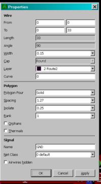
Spoke width is the track width used for the polygon pour.

Gap is set by the thermal isolate parameter in the DRC Supply tab.

Have a look at SPLIT and see if that helps your moving problem. It is difficult to know exactly what you are trying to move in what direction but you can pick up the 45 degree part and move that.

Keith
 
Hi Keith

It's not a bump, I had a question about CAM, but I found a Youtube instruction, so I tried to delete the question so you don't have to answer it. There is no delete complete post feature, so I just delete the words and put in some period.

I know how to set the isolation width of the thermal, I want to increase the spoke width but cannot find a way yet.

Thanks

Alan
 

As I said, spoke width is the track width used for the polygon pour. 0.15mm in this example.


Keith.
 
As I said, spoke width is the track width used for the polygon pour. 0.15mm in this example.


Keith.

Thanks

But the problem is if I change the wire width to say 25mils, the polygon fill does not work that well as the copper won't fill between pins. You'll get breaks in the copper plane. That's the reason I set it to 0.005 so it fill in the space between pins of 100mils spacing. I do use 18mils polygon isolation.

In OrCad, these are two separate parameters that I can set separately.

Thanks
Alan
 

Hi Keith

I ran DRC with the tStop on, there are quite a few error complaining the solder mask covering the part outline on tPlace and pads landing on the part outline. Can I ignore them?

I have another problem of the DRC where it complained about a 1 mil line on the copper polygon used as ground plane on the top layer. It always happen on the side of the copper at the board side. I tried moving the side away from the edge of the board and it did not help. I even delete the original copper and redrew a new polygon. The error is still there. What did I do wrong? I can't attach the board file as the attachment feature here does not accept a board file.

Thanks

Alan
 

I have a DRC problem complaining about the 1mil. I don't know what to make of it. Attached is the simplified board file, run the DRC and you'll see it at the bottom.

Thanks

Alan
 

Attachments

  • Test1.7z
    3.8 KB · Views: 40

Hi Keith

I ran DRC with the tStop on, there are quite a few error complaining the solder mask covering the part outline on tPlace and pads landing on the part outline. Can I ignore them?
They are when the silk screen overlaps the soldermask. Your PCB manufacturer may have a problem with it - I don't know. I have never had any problems.

If your silk screen overlaps a pad that is more serious (and is probably what the DRC should really be checking). My PCB supplier automatically clips the silk screen so it doesn't overlap pads so I don't tend to worry about that either. If you turn off the solder mask layer when doing the DRC you won't get the errors.

I will have a look at your other problem and get back to you shortly.

Keith

- - - Updated - - -

You have a 10mil minimum track width design rule and drawn the polygon with a 5mil track - hence the error. Change the width to 10mil.

I notice your polygon doesn't actually connect to any circuit nets.

Keith

Thank you very much, I did not see the update. I really appreciate all your help.

Alan
 

Status
Not open for further replies.

Part and Inventory Search

Welcome to EDABoard.com

Sponsor

Back
Top