tenso
Advanced Member level 4
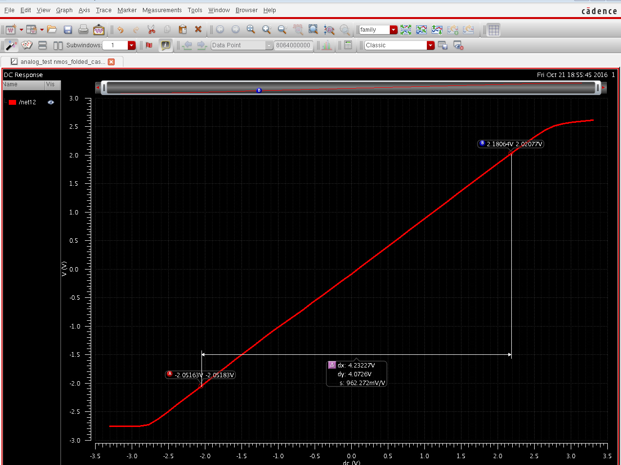
So I connected the folded cascode I designed in unity gain feedback configuration and swept the non-inverting input between Vdd and Vss to estimate my ICMR min and max. The graph is attached.
I then shorted both the inputs and connected them to a DC source supplying a voltage value (for a common mode voltage) within my ICMR range and then looked at the operating regions of my transistors.
I was under the impression that the ICMR is the range of values for which all devices should be in saturation. But for some region the branch with the current cascodes always seems to stay in cutoff. They hardly seem to seeing any DC current.
I took the current in the tail NMOS to be around 100 uA and the current coming from the PMOS transistors connected to VDD to be twice of that around 200uA. The PMOS transistors below them and the NMOS current mirrors were sized with the consideration that the entirety of the 200 uA flows through them (so maximum width). Still don't see any bias current flowing through them. The resistance seen looking into the lower PMOS transistors and the current mirrors seems to be huge.
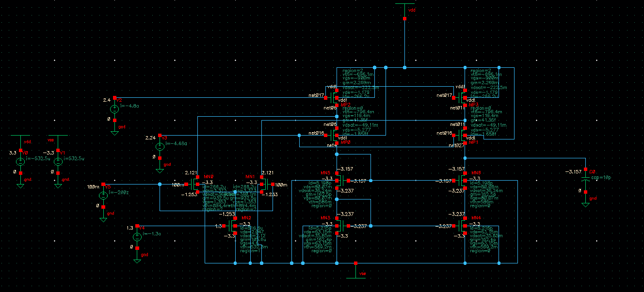
I have attached the schematic of my circuit.
Can someone help me out and point out what is going on ?
I then shorted both the inputs and connected them to a DC source supplying a voltage value (for a common mode voltage) within my ICMR range and then looked at the operating regions of my transistors.
I was under the impression that the ICMR is the range of values for which all devices should be in saturation. But for some region the branch with the current cascodes always seems to stay in cutoff. They hardly seem to seeing any DC current.
I took the current in the tail NMOS to be around 100 uA and the current coming from the PMOS transistors connected to VDD to be twice of that around 200uA. The PMOS transistors below them and the NMOS current mirrors were sized with the consideration that the entirety of the 200 uA flows through them (so maximum width). Still don't see any bias current flowing through them. The resistance seen looking into the lower PMOS transistors and the current mirrors seems to be huge.
I have attached the schematic of my circuit.
Can someone help me out and point out what is going on ?