Continue to Site

Welcome to EDAboard.com

Welcome to our site! EDAboard.com is an international Electronics Discussion Forum focused on EDA software, circuits, schematics, books, theory, papers, asic, pld, 8051, DSP, Network, RF, Analog Design, PCB, Service Manuals... and a whole lot more! To participate you need to register. Registration is free. Click here to register now.

question about Bandgap simulate

Status
Not open for further replies.

stoned

Member level 3
Joined
Feb 23, 2006
Messages
55
Helped
7
Reputation
14
Reaction score
2
Trophy points
1,288
Activity points
1,606
1/f noise and bandgap

Hi all:
The PM of the whole loop should be considered carefully to avoid oscillations.
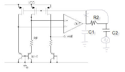
So I want to confirm it and get PM of the whole loop of my circuit by simulating. The figure as the following.
I break the loop at the Opamp output node, and add AC source series a capacitance at the gate of the top PMOS, and plot the Amp out node result. But the result is about -20dB of opamp output node. It’s right?
Can somebody give me the detail method of simulation to get PM?
Large signal stability:
I calculated the positive and negative feedback respectively, finding that positive is large than the negative, but the sum is small than unit.
When I ramp the Vdd from 0 to Vdd during 1ns, the BandGap will be stable after 3us, and with some ring during these time, so I think the phase margin is not enough, how to solve this problem? Add capacitance between out and ground?

Noise:
Does noise simulation required the noise model? When I use the following cmd to simulate.
vdd vdda 0 vol ac=1
.ac dec 10 .1 10
.noise v(vref) vdd
.print noise inoise

the result is
**** the results of the sqrt of integral (v**2 / freq)
**** total output noise voltage = 63.5984u volts
**** total equivalent input noise = 200.0866m volts
******

how to simulate the noise?
Thanks a lot!
stoned
 

how to simulate noise in bandgap

You understand that there are two feedback loops in the circuit.

Open the +ve FB loop at the input of the op-amp.Connect a DC source at that terminal (-ve, inverting i/p of op-amp) of the same value as the Operating point voltage of that point.

In the -ve FB loop (+ve or non -inverting input of the op-amp), insert a AC resistor (open in AC and short in DC) and a large cap (1F) at the input side of the op-amp.

DO the AC analysis and see the gain and phase at the point where the loop is broken (two loops).The gain of the +ve FB loop should be always be smaller than the gain at the -ve FB loop.
See the PM at the point where the -ve FB loop is open .ie before the AC resistance.

Regards,
Dhasmana.
 

    stoned

    Points: 2
    Helpful Answer Positive Rating
47_1175077301.jpg

I don't know how do you break the loop at the opamp output. I uaually break like this. C2 and R2 are large enough, e.g 1Mf and 1Mohm. C1 is the gate capacitance of pmos current mirrors.

The "ring" during startup is normal. There is always "ring" during startup.

Noise is necessary and the way you simulate noise is correct except for the frequency range which is too small.
 

    stoned

    Points: 2
    Helpful Answer Positive Rating
xuel said:
I don't know how do you break the loop at the opamp output. I uaually break like this. C2 and R2 are large enough, e.g 1Mf and 1Mohm. C1 is the gate capacitance of pmos current mirrors.

The "ring" during startup is normal. There is always "ring" during startup.

Noise is necessary and the way you simulate noise is correct except for the frequency range which is too small.
thank you for your help
I only want to get 1/f noise, so i selected the small range.
why i get so large value of noise, i doubted that the input large than the output!
 

In this case of bandgap, it's better opening the loop on both inputs and apply +0.5/-0.5 ac voltage source on it. It's the best way to simulate the PM/GM.

You can also use vcvs to really open the loop.
 

dreamteam said:
In this case of bandgap, it's better opening the loop on both inputs and apply +0.5/-0.5 ac voltage source on it. It's the best way to simulate the PM/GM.

You can also use vcvs to really open the loop.

Thank you very very much :)

now the noise simulation becomes the prime problem :(
 

Input noise is useless, because it is get from output noise devided by transfer gain from power to output. From your simulation, the gain (of psrr) is 60u200m=1/3000 or -70dB. For bandgap, we only need to care output noise.
 

dhasmana said:
You understand that there are two feedback loops in the circuit.

Open the +ve FB loop at the input of the op-amp.Connect a DC source at that terminal (-ve, inverting i/p of op-amp) of the same value as the Operating point voltage of that point.

In the -ve FB loop (+ve or non -inverting input of the op-amp), insert a AC resistor (open in AC and short in DC) and a large cap (1F) at the input side of the op-amp.

DO the AC analysis and see the gain and phase at the point where the loop is broken (two loops).The gain of the +ve FB loop should be always be smaller than the gain at the -ve FB loop.
See the PM at the point where the -ve FB loop is open .ie before the AC resistance.

Regards,
Dhasmana.

hi,why open the +ve and insert a dc source. there is no different with the origin circuit in terms of OP.
 

Status
Not open for further replies.

Similar threads

Part and Inventory Search

Welcome to EDABoard.com

Sponsor

Back
Top