Welcome to our site! EDAboard.com is an international Electronics Discussion Forum focused on EDA software, circuits, schematics, books, theory, papers, asic, pld, 8051, DSP, Network, RF, Analog Design, PCB, Service Manuals... and a whole lot more! To participate you need to register. Registration is free. Click here to register now.
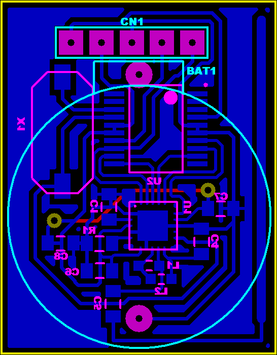
i m using 28 pin qfn package. in this, centre pad is the ground pin. how to ground this pin. if i routing this pin, error occurs. is it possible to add via in centre pad?
How do you know? Connecting the exposed pad may be strongly required, and thermal vias, too. For designs that have the pad connected to ground, routing the additional ground pins to it may be reasonable (unless a separate ground connection is suggested in the component datasheet). Getting errors with this connections is mainly an issue of the PCB library definition, and possibly a general problem of your layout tool.
This site uses cookies to help personalise content, tailor your experience and to keep you logged in if you register.
By continuing to use this site, you are consenting to our use of cookies.