Crazy8
Newbie level 4
Hi,
I am working on DC-DC Flyback converter and have been facing a serious problem of MOSFET failure due to over heating.My desire task is to achieve output Power in range of minimum 20W-30W at-least.
But in range of 5 to 8W Max of power (both in and out), MOSFET starts heating that causes failure which is limiting my converter to be operated in very low power and stopping me to increase to required power level.While figuring out the problem or reasons of MOSFET failure the main point is MOSFET break down voltage region that is 650V drain voltage.In my case it fails in range of 150V drain voltage,Iin 320mA, 25V Vin at transformer Primary.
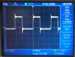
If we have a look on PWM issues, my PWM is jitter free but having ripples at rise and fall.can this be a reason of this problem if we take in to consideration while figuring out the problem, then how can i remove them.
MOSFET=IPL60R385CP CoolMos
I would appreciate the suggestions and guidance.
Thanks

Last edited: