Continue to Site

Welcome to EDAboard.com

Welcome to our site! EDAboard.com is an international Electronics Discussion Forum focused on EDA software, circuits, schematics, books, theory, papers, asic, pld, 8051, DSP, Network, RF, Analog Design, PCB, Service Manuals... and a whole lot more! To participate you need to register. Registration is free. Click here to register now.

Push-Pull Converter MOSFET Issue

Status
Not open for further replies.

Ungie

Newbie level 5
Joined
Jan 23, 2017
Messages
9
Helped
0
Reputation
0
Reaction score
0
Trophy points
1
Activity points
106
Hi Everyone,

I am working on a push-pull converter design for a small audio power amplifier. It converts incoming 15VDC from an external power supply to +/-30VDC. The supply works very well on the bench and all switching waveforms are clean. One issue that we have had is that sometimes on power up (SD is switched to 15VDC to enable) one or both MOSFETs will fail shorted G-S. What is strange is that this issue is completely un-repeatable and seems to occur at random. Could anyone point me to any areas where I should be looking? I should note that the turn on power requirement at the outputs of the supply are less than 300mA per rail, so I don't believe it is any sort of inrush issue.

Thank you!View attachment PP_SMPS.pdf
 

Hi,

I see two issues:
* there is no overvoltage protection across Mosfet DS.
* there is a capacitor in the SD circuit. This capacitor is initially discharged, 0V. But this means the bjt is high impedance.
The driver_SD is high, means the driver is active.
--> I recommend to put the capacitor across EC (instead BE).

Klaus

Thank you Klaus,

Note that there is one error in my schematic...the centre-tap of the transformer primary is 15V, not 12V as marked. The MOSFETs used have a Vdss of 75V and the input will never exceed 15V. Is D-S overvoltage protection really necessary here? Is it required because of any transient at turn-on? Do you suggest a TVS? Understood about the SD circuit...could this be causing some sort of MOSFET latch-up when power is applied? The normal start condition is that +15V is present everywhere that is noted and upon pressing a power button, SD is brought to +15V to enable switching. I'm still baffled that these MOSFETs are randomly being killed...

Thank you!
 

I also killed several mosfets as I tried to make a power inverter with a center-tap primary (principle of operation like your design). I started getting large spikes as I continued to increase power through the unit. It is typical of inductors to create high voltage spikes when you shut off current through them. I didn't know enough about snubbing techniques. I gave up on the project. In addition I was using a transformer in reverse direction. It was designed to step down house AC to several lower voltages. Although it could step up 12V to high VAC, I was disappointed at the small power it provided.
 

It may very well be an over voltage problem, and some means of clamping drain voltage spikes should fix it, if that is the problem.

But there is a quite different possibility that it could be caused by an over current spike from magnetic saturation of the transformer.
This can be caused by flux doubling. When power is removed, there can be a residual magnetism remaining in the core. If at turn on, the switching direction drives the core in the same magnetic direction, it may saturate producing a huge current spike.

What is the design flux swing in the core ?
Does your circuit have peak current limiting or a soft start ?
 

Mosfets are notorious for their sensitivity to static charge and voltage spikes. The gate easily gets perforated, ruining the component.
 

It may very well be an over voltage problem, and some means of clamping drain voltage spikes should fix it, if that is the problem.

But there is a quite different possibility that it could be caused by an over current spike from magnetic saturation of the transformer.
This can be caused by flux doubling. When power is removed, there can be a residual magnetism remaining in the core. If at turn on, the switching direction drives the core in the same magnetic direction, it may saturate producing a huge current spike.

What is the design flux swing in the core ?
Does your circuit have peak current limiting or a soft start ?

Thank you Tony!
In order to determine if an over-voltage spike is responsible for randomly killing these MOSFETs, what would the preferred drain voltage clamping method be for this type of design? The transformer used, wound on a toroid core, was designed with a large amount of headroom and saturation is highly unlikely. I will confirm this with the transformer supplier. The amplifier that is powered by this supply has both peak current limiting and a soft start. The power supply itself has no current limiting and the soft start consists only of the SD control.

Thanks!
 

I suppose the first thing would be to look at the voltage waveforms with an oscilloscope.
Voltage spikes will either be there, or they will not be there.
How savage the spikes are, will determine how much power needs to be clamped, maybe very little ?

Toroids can saturate particularly suddenly, but check the voltage waveforms first.
 

The sg2525 data sheet has little information on soft start. They show one circuit with a 5uF cap on soft start term 8 but give no guidelines on how to calculate time. I would say you should use the oscilloscope to measure this time.

Also your shut down signal does not show were it connects to. If it is somewhere off the schematic past the secondary you loose your isolation. Also the shut down is working through a 12K to charge a 33uF, taking a long time to be of much good. The shut down is supposed to measure the current of your mosfets to stop them from burning up and be lightning fast.

But this is not a fix for a poor design that may have flux doubling problems. Try to get the whole design sheet for the transformer. Ferrite type, core used, number of turns.
 

I only just now realized there was a schematic in the first post.

First, the soft start is very slow, my own experiences with that chip suggest several seconds for 22uf, which is extremely gentle and slow.

Next observation is that there is no filter choke between the output bridge rectifier and the output capacitors, that is a VITAL component to limit current inrush into the output capacitors, it must be there for a push pull forward inverter, especially at startup.

Last, the error amplifier seems to be tied to produce maximum output duty cycle without any voltage feedback from the output.
That in itself is pretty unusual, because the dc output voltage is essentially unregulated.
 

Thank you everyone for your input so far, I appreciate you all stepping in to assist a newcomer to these forums!
I have spent some time thinking about conditions where this is happening and also had a much closer look at the startup waveforms on the MOSFETs. I should note that, in case it was not clear above, this power supply works flawlessly under all load conditions and the actual switching waveforms are all very clean. In cases where the MOSFETs are damaged it is ALWAYS upon starting the supply, i.e. applying 15V to the SD control point. It has never occurred when simply applying 15V to the other points in the circuit. So, main power (B+) is already on. When 15V is applied to SD, the signal on the MOSFET gates looks nice and clean with no spikes that I can discern. The drain, however, is another story. I am seeing spikes before actual switching startup has stabilized that might be approaching the Vdss limit. So it is looking like it is certainly possible that this could kill a MOSFET under some conditions. So, my next question is what are the favored methods for clamping the drain to limit Vdss to well within safe limits? I have seen anode to anode diode+zener, TVS, etc. I am not particularly familiar with these methods, so any pointers would be most appreciated. Also, these MOSFETs have a maximum Vgs of +/-20V and this circuit is running with a gate switching voltage of 15V, so it would probably be a good idea to also apply some clamping to protect the gates. Thoughts if this is necessary?

To Warpspeed: I have encountered many existing designs using SG2525 or SG3525 where there is no filter choke after the output bridge. I order to save costs and space, I have omitted them from this design. However, if it is best practice to include them I will revisit the topic. I am running this power supply unregulated, as the load is not sensitive to precise rail voltages and will tolerate rail sag under higher load conditions.

Thanks!
 

Hi,

A simple zener without additional diode across each Fet DS.
One problem could be the relatively high capacitance of zeners and if you have high dV/dt.

Klaus
 

In addition to the flux doubling issue, it could also be staircase saturation.
If the opposite legs of each transformer and all the components attached to it are not identically matched, the one side will receive slightly more volts seconds each cycle, with the remanence flux slowly "walking the stairs" towards saturation....until it destroys itself.

There is information on the web....please google the term.

Unfortunately, the SG3525 does not have an effective means of flux balancing, it is a very old, very simplistic design.

A far better, push-pull current mode controller is the LM5030. It has pulse by pulse current limiting.
 

Schmidt trigger raises a very important issue.
Staircase saturation used to be a very common with poorly matched components in push pull topology, its particularly bad with bipolar transistors and centre tapped single primary and secondary windings.

These days with mosfets and bifilar winding techniques, and current mode control chips, it has become much less of a problem.
But if you do not know about this staircase saturation effect, it is something you should research.
Once you understand what causes it, you will very quickly know if its likely to be the problem.
 

In addition to the flux doubling issue, it could also be staircase saturation.
If the opposite legs of each transformer and all the components attached to it are not identically matched, the one side will receive slightly more volts seconds each cycle, with the remanence flux slowly "walking the stairs" towards saturation....until it destroys itself.

There is information on the web....please google the term.

Unfortunately, the SG3525 does not have an effective means of flux balancing, it is a very old, very simplistic design.

A far better, push-pull current mode controller is the LM5030. It has pulse by pulse current limiting.

Thank you. I am looking into staircase saturation, but what I am seeing so far would suggest symptoms happening during operation. It is possible that this effect could occur immediately after pulling SD low?
 

Schmidt trigger raises a very important issue.
Staircase saturation used to be a very common with poorly matched components in push pull topology, its particularly bad with bipolar transistors and centre tapped single primary and secondary windings.

These days with mosfets and bifilar winding techniques, and current mode control chips, it has become much less of a problem.
But if you do not know about this staircase saturation effect, it is something you should research.
Once you understand what causes it, you will very quickly know if its likely to be the problem.

Thank you Warpspeed...much appreciated!
In my case the supply design is using MOSFETs and a bifilar wound toroid transformer. Current requirements from the load are fairly low and the supply works without issue into no load and load conditions beyond what it will ever see in operation. I'm not understanding why this low-tech design should be an issue. The symptoms of MOSFET destruction now seem to clearly point to a start up transient issue, but I of course am no expert in this field. I think for now I will try applying zener protection to both the gates and drains on my prototype and see if it continues to randomly damage MOSFETs. I'll also have a look at the LM5030 and see how it would compare from a cost/performance standpoint.

Thanks!
 

To understand about saturation effects, we should know the core type and flux in regular operation.

A push-pull transformer without any clamping or snubber might drive the MOSFET into avalanche breakdown in regular operation. Inrush current during output capacitor charging will cause respectively higher avalanche energy which might be sufficient to kill a MOSFET. One would look a Vds waveforms to understand if clamping is required.

Thank you FvM. Here are the transformer specifications:

Core

Toroidal Code
Ferrite F Material
Epoxy Coated (200 degC breakdown)
O.D. 31mm
I.D. 19mm
H 13mm

Winding Structure

Interlaced windings
Primary 1 8 turns, 2 x 1.12mm(18 AWG) copper (bifilar wound), clear insulated coating
Primary 2 8 turns, 2 x 1.12mm(18 AWG) copper (bifilar wound), red insulated coating
Secondary 1 19 turns, 1 x 1.12mm(18 AWG) copper, clear insulated coating
Secondary 2 19 turns, 1 x 1.12mm(18 AWG) copper, red insulated coating
1:2.375 turns ratio

The only reason I have not applied snubbers is because Vds is extremely clean with very little ringing or overshoot. In this case I did not think it required.

Thanks!
 

If I calculated right, you have about 160 mT Bpk in continuous operation. Due to soft start feature, there won't be any higher flux during start-up.

Did you record waveforms during startup?

- - - Updated - - -

The only reason I have not applied snubbers is because Vds is extremely clean with very little ringing or overshoot. In this case I did not think it required.
This might be if you very good coupling between primary windings.
 

If I calculated right, you have about 160 mT Bpk in continuous operation. Due to soft start feature, there won't be any higher flux during start-up.

Did you record waveforms during startup?

- - - Updated - - -


This might be if you very good coupling between primary windings.

Hi FvM,

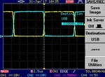
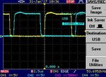
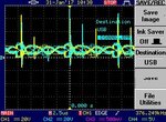
I have attached scope captures of the gates and drains while the supply is running and also the drains during the initial startup condition. You can clearly see spikes from 60-80V. This could always be induced noise in my scope probes/leads, but I am thinking it is probably a good idea to add both Vds and gate protection zeners.

Thanks!

Drains_Startup.jpgDrains.jpgGates.jpg
 

Status
Not open for further replies.

Part and Inventory Search

Welcome to EDABoard.com

Sponsor

Back
Top