Continue to Site

Welcome to EDAboard.com

Welcome to our site! EDAboard.com is an international Electronics Discussion Forum focused on EDA software, circuits, schematics, books, theory, papers, asic, pld, 8051, DSP, Network, RF, Analog Design, PCB, Service Manuals... and a whole lot more! To participate you need to register. Registration is free. Click here to register now.

Pull Down Network after PMOS Power Switch for two inverters connected in series

Status
Not open for further replies.

tarjina

Junior Member level 3
Joined
Jun 7, 2012
Messages
30
Helped
0
Reputation
0
Reaction score
0
Trophy points
1,286
Activity points
1,536
Hello everyone. I am simulating a very easy circuit with CMOS. It has two pMOS power switches. Each connected to two inverters in series. The circuit looks like below:
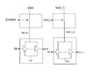
inverter.jpeg

So, when the Enable is low, the output should follow input and when enable is high, we are cutting off the power so the output should be low (I need low, not the previous state).
so I need a pull down network. But, the problem is I cannot connect a resistor to the vdd_internal. Because, we can not touch the layout.
Now, I have created a test bench to test this circuit. It looks like below:
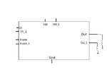
tb.jpeg

now, how can I insert the pull down network in this testbench? or any other ideas to pull down the vdd_internal to 0 when the power supply is OFF?
Thanks in advance.
 

If you're only simulating, you don't need to touch the
layout. Do what you need to.

Now, in the de-powered state, all you care about is the
two outputs, so maybe it's enough to hang the loads
there. You could be a bit clever and make an opposite
state (on, when power is cut) NMOS shunt pair instead,
giving no wasted current in normal operation and a much
lower layout area.
 
Sorry, I did not get your point. Actually I will have to simulate a bigger circuit later. This is the startup. So, all I can do is making testbenches. so, Did u mean adding NMOS shunt pair at the output?

- - - Updated - - -

Okay, so I add two NMOS to the output, but the output curves look ugly. :(

bank_m2_tb_Load_NMOS.jpg

Any idea, how to make them smooth?
 

The pmos devices will cut the flow of current to the inverters, but this does not allow the outputs to pull low. If you want the output to be 0 volts you will need an nmos shunt device on the outputs. When enable is high, the pmos devices will cut the current flow to the inverters, and the nmos devices will turn on, pulling the outputs low. Alternatively, you could avoid tristate circuits by AND'ing the input signal with a high-asserted enable...
 
Okay, so does the shunt connection look like below?

schematic.jpeg

But this is not giving me a smooth curve. You can see I have an internal Vdd of 220mV when it is supposed to go to 0mV. since my supply power is 800mV, 220mV is a real concern for me.

schematic_op.jpg

Please help. TIA
 

Not diode connected MOS - regular common source MOS
switches with the gates running off the enable input of
the block (or, inverted, depending on the sense of the
enable input). If enable is active high, then invert before
the NMOS gate.
 

Yeah, I figured that out. Just showed it to my Supervisor. But he said, I can not use MOSFETs there. Need to do something with Resistors.
Any idea?

- - - Updated - - -

Nevertheless, the shunted NMOS switches smooths the output, it does not pull the internal Vdd to 0 :(
 

This must be an exercise without real value, because a
MOS shunt always is more compact ($) than a resistor
and also less power wasted.

So hang resistors where you had those MOS diodes and
call it done, I guess - although maybe proposing the more
efficient alternative as well, could get you extra credit
or at least a better grade.
 

Status
Not open for further replies.

Similar threads

Part and Inventory Search

Welcome to EDABoard.com

Sponsor

Back
Top