Continue to Site

Welcome to EDAboard.com

Welcome to our site! EDAboard.com is an international Electronics Discussion Forum focused on EDA software, circuits, schematics, books, theory, papers, asic, pld, 8051, DSP, Network, RF, Analog Design, PCB, Service Manuals... and a whole lot more! To participate you need to register. Registration is free. Click here to register now.

Protecting FETs from CEMF spikes

Status
Not open for further replies.

Kerrowman

Member level 4
Joined
Oct 12, 2021
Messages
75
Helped
0
Reputation
0
Reaction score
2
Trophy points
8
Location
West Penwith
Activity points
578
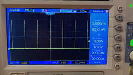
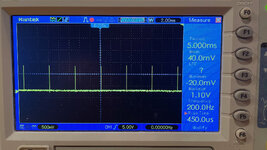
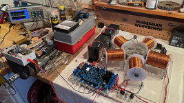
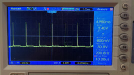
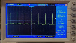
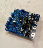
In my doing some research into the effects of HV CEMF pulses on batteries, I am finding that my MOSFETs understandably get easily damaged by these pulses, even when I have tried to isolate and protect them using a pair of chokes (see pic).

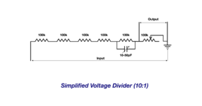
I also attach the relevant part of the circuit and wondered if anyone had any straightforward ideas as to how to block the CEMF pulses (~ 1,200V) from reaching the FETs? Maybe a fast diode between the Drain and Source of each one? However, the Source does not connect to Ground but supplies another part of the circuit.

Thanks

Chokes.jpg

FET Protection.jpeg
 

Interesting- from what you say I should either reduce the voltage to the Gate, say to 6V, so that Vgs is significantly greater than the Vgs (th) or do without the FETs altogether. When I considered the latter some years ago I thought that the small relay was not up to switching 2A securely.

I should probably build a small vero board circuit to test the idea out.

The swapper worked with its high sided switching using the TIP3055 but off the top of my head I’m not sure why.

I suppose another option would be to switch to P channel devices and use the relay to ground the Gate and turn them fully on that way - bit like I’m using in part of my cap dump circuit to route the ensuing cap discharges.

However, since it seems the relay can switch 3A I will have a go at just using that. I’ll save a lost volt or so as well 😊
 
Last edited:

I think it should be the other way around, you need MORE voltage on the gate to reduce the effective resistance of the MOSFET. Try just the relay, I suspect when you used the TIP3055 it was because the B-E junction carried most of the current.

The only way to maintain the 12V on the drains while pulsing the batteries is to add the chokes as you have done. The easiest way to maintain the drain voltage at safe levels is to add a Zener diode between the drain and 0V line so the DC path is still relying on the chokes resistance but it's inductance blocks the spike. If you use a Zener rated at say 15V or 18V it should keep the MOSFET safe.

Brian.
 

Hi Brian,

Yes I will certainly try just using the relay and no FETs.

The reason for having a swapper at all is so that the battery providing all the power is not being pulsed at the same time with the HV spikes or, in due course, the high current capacitor discharges. The one being pulsed is otherwise idle. If it were otherwise then there would indeed be issues of keeping the 12V stable at the Drains.

Also batteries don’t seem to like delivering energy, with the corresponding chemistry changes, while also trying to respond to incoming impulses. Bit of a push - pull situation. Another reason for the swapper.

Without the FETs I surely then won’t need the chokes as there is nothing to protect anymore. I will draw it up and post soon anyway.
--- Updated ---

Here is a revised swapper with no FETs at all. This should be ok for a low power rig where the total current is <2A. This certainly gets around any topology issues as FvM outlined.

Battery Swapper (No FETs).jpeg
 
Last edited:

Yes, using just the relay works a treat 😊 Thank you all for your suggestions. Onwards now with the cap dump and revised voltage divider.
 

Hi all,

Over the last week or so I have been working on calibrating the updated potential divider that uses 100k resistors and includes a cap trimmer for probe compensation (Pic 1).

Early tests using DC and square wave calibration waveforms and voltages were helpful in setting the compensation and getting a sharp square waveform but seemed to give very inaccurate results (182V) since the HV spikes have a 10-20us rise time and the calibration inputs are very different from this. So I decided to use a calibration waveform similar to what I will be actually measuring in the form of a 10V 'impulse' waveform from my signal generator as shown in Pic 2. Using this I set the divider's adjustment pot to give a value as close to 10V/10 as I could get which was in fact 1.1V (Pic 3) and which amounts to a divider ratio of 9.1:1 (the probe compensation had been previously adjusted to give sharp square corners using a CMOS waveform input).

Pic 4 shows the measurement setup and Pic 5 the measured HV spike peak voltage at 80.8V=735V compared to the previous DC/CMOS calibration (Pic 6). This new value is consistent with others who are doing similar work in other countries where 500-1,000V is the norm.

The actual peak value of the pulses is not important in itself. The only significance of having a high value is that it will charge up the large storage capacitors faster and which will then dump their charge into the batteries at a higher rate. This 'cap dump' part of the circuit is currently under construction (Pic 7) with its heavily beefed-up conduction tracks.

I also found that bypassing the FET driver produced spikes of the same value as with it and so my design decision to incorporate it to reduce the FET shut-off times (V = -L dV/dt where if dt is shorter then the CEMF will be greater) was either not effective or some other factor is masking the increase.

So a lot has been learned during this interesting detour and some interesting questions have arisen out of it:

1. What is it about the use of short-duration 'impulse' inputs that changes the way the divider works compared to DC or the relatively long duration of square waves - possibly frequency-related impedance changes?

2. What might be masking the increase in the spike voltage arising from using a FET driver? (To avoid mudding the issues in this post I will show my ideas on this in a subsequent post).

Thanks
 

Attachments

  • Pic 1 - Adjustable Potential Divider (10-1).png
    Pic 1 - Adjustable Potential Divider (10-1).png
    135.7 KB · Views: 67
  • Pic 2 - Divider input using 'impulse' input.jpeg
    Pic 2 - Divider input using 'impulse' input.jpeg
    698.1 KB · Views: 64
  • Pic 3 - Divider calibration using 'impulse' input.jpeg
    Pic 3 - Divider calibration using 'impulse' input.jpeg
    694.3 KB · Views: 64
  • Pic 4 - Measurement setup.jpeg
    Pic 4 - Measurement setup.jpeg
    982.2 KB · Views: 63
  • Pic 5 - Revised HV measurement.jpeg
    Pic 5 - Revised HV measurement.jpeg
    718.7 KB · Views: 64
  • Pic 6 - Divider adjusted for DC and CMOS wave.jpeg
    Pic 6 - Divider adjusted for DC and CMOS wave.jpeg
    707.2 KB · Views: 68
  • Pic 7 - Cap Dump Build.jpeg
    Pic 7 - Cap Dump Build.jpeg
    1.4 MB · Views: 67

Status
Not open for further replies.

Similar threads

Part and Inventory Search

Welcome to EDABoard.com

Sponsor

Back
Top