Continue to Site

Welcome to EDAboard.com

Welcome to our site! EDAboard.com is an international Electronics Discussion Forum focused on EDA software, circuits, schematics, books, theory, papers, asic, pld, 8051, DSP, Network, RF, Analog Design, PCB, Service Manuals... and a whole lot more! To participate you need to register. Registration is free. Click here to register now.

Problem with the Bandwidth of switched capacitor

Status
Not open for further replies.

mashnayn

Newbie level 4
Joined
Jul 10, 2011
Messages
5
Helped
0
Reputation
0
Reaction score
0
Trophy points
1,281
Activity points
1,359
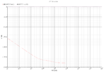
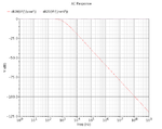
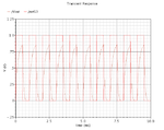
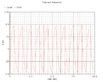
Hi everyone i am designing a simple integrator using Switched capacitor, the clock frequency of which has been chosen as 100KHz and the Rsc=1K ohm and capacitor value of 15nF as shown in the circuit.The problem here is the bandwidth of the system has been reduced drastically though the output is being integrated properly, please suggest me the solution behind this problem. Actually in case of Switched capacitor integrator the bandwidth will be more than that in the case of ordinary RC-Integrator,but i am getting reverse effect.
 

Attachments

  • Bandwidth of SC integrator.png
    Bandwidth of SC integrator.png
    11.4 KB · Views: 205
  • RC integrator BW.png
    RC integrator BW.png
    5.4 KB · Views: 197
  • RC integrator.jpg
    RC integrator.jpg
    37 KB · Views: 174
  • snapshot1.png
    snapshot1.png
    12 KB · Views: 156
  • snapshot12.png
    snapshot12.png
    13.7 KB · Views: 167
  • switched capacitor.jpg
    switched capacitor.jpg
    65.3 KB · Views: 223
Last edited:

I think, some comments are necessary:
* At first, a simple RC combination is not an integrator but a first order lowpass
* Replacement of a resistor by a switched cap is allowed only if BOTH sides of the resistor are connected to a voltage source or ground (for example: opamp inverting input because of virtual ground properties).
* AC simulation of a time discrete circuit requires some "tricky" measures resp. specific program features. Which simulator do you use?
 

LvW.. I know what you mean by its a first order lowpass, but it can also be considered a lossy integrator.

As for the integrating part, I would say you are clipping in your integration plots.. What are you supplies? Also, test it with a smaller square wave to see a nice triangle wave, thus a nice integration.

jgk
 

Replacement of a resistor by a switched cap is allowed only if BOTH sides of the resistor are connected to a voltage source or ground (for example: opamp inverting input because of virtual ground properties).

Supplement: As an approximation you can treat the most right (load) capacitor as a voltage source - if it is much larger than the switched capacitor.
 

Hi thank you for the reply, coming to simulation tool that iam using is CADENCE Virtuoso.As can be seen in the switched capacitor integrator circuit, the input to the circuit has been given as a pulse signal, and the mosfets are being supplied by non-overlapping pulse signals of 100kHz frequency which will give a resistance of 1K ohm.

when you mean by small square wave, what actually does it mean..?,small in the sense what..?
The main problem here is Bandwidth of the switched capacitor low pass or integrator circuit is very less than its actual BW.Actually it should have been 1061Hz but in my case i am getting 13 Hz as Bandwidth, please help me in this regard...
Thank you...

---------- Post added at 17:58 ---------- Previous post was at 17:52 ----------

Hi thank you for the reply, the simulation tool i am using is CADENCE virtuoso. I didnt get the second statement what you were mentioning, replacement of a resistor by a switched capacitor is allowed by both sides of the resistor are connected to a voltage source or ground

As you were mentioning a simple RC combination is not an integrator but a first order low pass, can't it be treated as an integrator ?
and when it is working as a low pass filter giving some bandwidth of 1061Hz, when the same low pass circuit is being simulated using switched capacitor concept why the bandwidth is getting reduced drastically from 1061hz to 60hz ?
Please help me in this regard
Thank you

---------- Post added at 18:03 ---------- Previous post was at 17:58 ----------

what kind of tricky measures do i need to follow when simulating time discrete circuits
 

Hi again,

some more comments:

* You have designed a 1st order lowpass (damped integrator) with a corner (3-dB-frequency) of approx. 10 kHz (R=1k, C=15nF)
* That means: Approximate integration can take place for frequencies much larger than 10 kHz only - let's say, for example, for f>100 kHz.
* This requires a clock frequency that is larger than the operating signal frequencies by at least a factor of 50...100.
* Example: Fclock=10 MHz
* Requirement: The time available to charge/discharge the capacitior (10 nF) must be at least (2...3)*Tclock - resulting in a switch resistance Ron<10 ohms.
__________
The above example gives you some basics to play with parts values and clock frequencies with the aim to design a working circuit.
However, please consider that a good SC integrator can only be designed using an opamp.

Two additional points:
*What do you mean with "bandwidth, actually it should have been 1061Hz". How did you arrive at this value? What is it's relevance?
*As far as ac analysis is concerned: From the definition point of view an ac small signal analysis is possible for time continuous systems only.

---------- Post added at 22:04 ---------- Previous post was at 20:40 ----------

Supplement: However, an ac analysis is, of course, possible. For this purpose the time discrete circuit is transferred into a time continuous system. This can be done using appropriate simulation programs (perhaps SPECTRE?) or some other "tricky" time continuous equivalent units replacing each SC unit.
 
Thank you again for the reply, first i will give the answers for the questions what you have posted :
"Two additional points:
*What do you mean with "bandwidth, actually it should have been 1061Hz". How did you arrive at this value? What is it's relevance?
*As far as ac analysis is concerned: From the definition point of view an ac small signal analysis is possible for time continuous systems only"

(1)In the lossy integrator schematic the value of R=1K ohm, and C=150nF, which gives a bandwidth 1/2pi(RC) which gives a value of 1061 Hz in my case, where as when the same circuit is being implemented using Switched capacitor circuit with the same values,(here input signal is of 1KHz, clock frequency has been chosen 50 times or 100 times of input frequency,hence of value 100kHz,with C=10nF,and load C=15nF as can be observed from the schematic, should give a bandwidth of 10610Hz (since R will be here 1000ohms and c=15nF) I am not getting the correct bandwidth

whats wrong in my concept, can i actually replace the lossy integrator circuit using switched capacitor integrator circuit or not
(2) when i am simulating the switched capacitor circuit which is actually discrete time signal, using Cadence virtuoso,what precautions should i take to get exact results, i mean can i still use ac analysis

Thank you once again
 

Hi mashnayn,

here is my answer:

To (1): With R=1k and C=150 nF you have a lowpass with a 3-dB corner of 1061 Hz. As mentioned before, this circuit can act as an integrator only for frequencies far above this frequency (because of the required phase shift of approx. 90 deg).
How can you say " I am not getting the correct bandwidth"; what does it mean: "getting" ? Is this a result of hand calculation, measurement or simulation?
More than that, I have told you that you cannot expect to get an S/C integrator by simply using a passive RC lowpass and replacing the R by switched C. Theory tells you that such a replacement is allowed between voltage sources (or ground) only. Why do you ignore this information?

To (2) I am not familiar with Virtuoso. Consult the help feature or the handbook for information regarding ac simulation of time discrete circuits.
As I have told you already in my last answer: There are some rules and methods to transfer time discrete units into time continuous equivalents, which are suitable for ac simulation (periodic transfer function according to the DFT).
 
Mashnayn,
in RC cell, the capacitance is 150nF, which corresponds to the time constant RC=150us and the cutoff frequency of 1.06 kHz.
In SC cell, the capacitance is 15nF, which corresponds to the time constant RC=15us and the cutoff frequency of 10.6 kHz. Since the switching frequency is only 100kHz, it is only 10x more than the filter BW.
I do not understand why you have chosen two different values of C, and then you still compare the properties of these circuits. I only guess that you did a mistake and that the capacitance should be 150nF in both circuits.
I recommend you to check if your SC filter works in the time domain, i.e. via TRANSIENT analysis, under the sinusoidal excitation. I guess that there can be problems with improper operation of your MOS switches.You should check if they switch on and off properly.
Before many years, I constructed a lot of such SC filters from discrete components, also your simple LP filter. It worked well. The rule
"Replacement of a resistor by a switched cap is allowed only if BOTH sides of the resistor are connected to a voltage source or ground "
need not be fulfilled. The switched capacitor works as floating resistor if its both outlets are connected either to low-impedance nodes or capacitive loads.
I have also some simple simulation program, particularly for the AC analysis of SC filters which I made for my needs. If necessary, I can do an analysis of your circuit, taking Ron switches into account, for a comparison.
 

    V

    Points: 2
    Helpful Answer Positive Rating
.............
Before many years, I constructed a lot of such SC filters from discrete components, also your simple LP filter. It worked well. The rule
"Replacement of a resistor by a switched cap is allowed only if BOTH sides of the resistor are connected to a voltage source or ground "
need not be fulfilled. The switched capacitor works as floating resistor if its both outlets are connected either to low-impedance nodes or capacitive loads.
.

Hi Dalibor,

I like to comment your claims regarding "capacitive load".
In my former posting (#4) I have mentioned that a capacitor can act as a rough approximation of the required voltage source (or ground) only under the condition that it is much larger than the switched capacitor. Therefore, your above statement does not help at all without mentioning the capacitor ratios you have used.
More than that, you should be careful with statements like "...need not be fulfilled". A requirement that needs not to be fulfilled for proper circuit operation is no requirement!
Let me try to explain the situation based on a worst case scenario:
(1) If the "load capacitor" C2 is much smaller than the switched cap C1 it is clear that C2 cannot be discharged and, thus, will nearly keep its charge (and voltage). As a consequence, the charge transfer ("current") will be nearly zero.
(2) In case of two equal capacitors values the first one (C1) will be charged with a voltage V1 and - after transfer to to C2 - the resulting output voltage will be 0.5*V1. Thus, the output voltage suddenly jumps to half of the final value. Certainly not a good approximation to an RC behaviour.
(3) You can continue these examples for increased C2 values - and you will see that the best approximation to the analog circuitry requires a capacitor C2 that is very large if compared with C1 (optimum case: C2 infinite, which is identical to zero voltage).
_________________
More than that, you have claimed that your circuit "worked well". I suppose, you have used a buffer amplifier at the output (to decouple C2), didn't you?
Why not use this amplifier to build an active S/C circuitry without the above described disadvantages and error sources?
Therefore, I can see absolutely no reason for using a passive RC combination as a starting point for a switched-capacitor combination, which never can reach the exactness of an active realization.
Thank you
Regards
LvW
 

LwH,
OK, let us make the things clear.
After studying your comments, I (perhaps) found the reason why you defend the mistaken thesis

(T)"Replacement of a resistor by a switched cap is allowed only if BOTH sides of the resistor are connected to a voltage source or ground"

which was completed by the statement that

"a capacitor can act as a rough approximation of the required voltage source (or ground) only under the condition that it is much larger than the switched capacitor".

The word "required" in the additional statement underlines that you insist on the fundamental importance of the above thesis (T).
My response was that "The rule .. need not be fulfilled". Note that it is a diplomatic form of the message that your thesis is wrong.
In fact, the switched capacitor C1 simulates approximatively a conventional resistor, but the "accuracy" of this approximation will not be improved after connecting the terminal to ground or to low-impedance node.
Let me explain it.

How would you solve the following task: designing first-order lowpass filter with the cutoff frequency w0, described by the transfer function
K(s)=1/(1+s/w0),
via SC technique?
Mashnayn called it "integrator" but jgk2004 noted correctly that it is first order low-pass filter, or also a LOSSY integrator.
There are two basic possibilities of the synthesis of such SC filter:

(a) as passive SC filter, designed from passive RC prototype.
(b) as active SC filter, designed from active RC prototype.

Both methods are well-described in classical textbooks (for example, in the well-known monography by Ghausi and Laker [*]).
Mashnayn used the first approach. In [*], the switched C1 is described as floating Toggle-Switch Capacitor - TSC, creating together with C2 (of arbitrary capacitance) a "passive-SC First-Order Low-Pass filter" with the z-domain transfer function, being dependent on the ratio C1/C2. This ratio determines the -3dB cutoff frequency of the filter. There is no reason why to be angry at Mashnayn that he selected a circuit which does not match your thesis (T).
The second approach can be solved as active-SC lossy integrator. There are several schematics but all of them have the same starting point: classical RC active lossy OpAmp-based integrator with additional resistor in parallel to the feedback capacitor. For equal resistances of both resistors in the circuit, the transfer function is the same as for passive RC cell (except for the inversion property of active circuit).
If both resistors are replaced by their TSC equivalents, you obtain active-SC lossy integrator with TSC damping [*]. Both switched capacitors are in full accordance with your thesis (T) since they switch to the OpAmp virtual ground. According to your belief, you should expect that this circuit will represent "better approximation" of the required analog filter than Mashnayn passive TSC filter which works to C2.
However, if you compare the frequency characteristics of both implementations with "ideal" characteristics of the analogue prototype, you find the following:

For [C1, C2] = [10, 150]nF, f-3dB for analog filter is 1.06 kHz.
f-3dB for passive SC filter is 1.03 kHz,
f-3dB for active SC filter is 1.1 kHz.

For [C1, C2] = [10, 15]nF, f-3dB for analog filter is 10.6 kHz.
f-3dB for passive SC filter is 8.3 kHz,
f-3dB for active SC filter is 19.5 kHz.

As you can see, for C2>>C1 (the case which you consider as necessary for proper function of passive SC filter), both SC filters work well, and their cutoff frequencies (which depend indirectly on the simulated R) correspond to the "ideal" value.
However, for C2=1.5*C1 (the case which you consider as "bad approximation" for passive SC filter but not violating the operation of SC resistor with grounded outlet), both filters exhibit declinations from the anticipated cutoff frequencies, but the active filter brings much bigger error to the simulated resistance.
The explanation is as follows: these errors have nothing to do with the way of the termination of switched capacitors. They are governed by the s-z approximation which is given by the type of SC circuit for simulating the resistor (for example, TSC circuits lead to the so-called FD (forward-difference) integrator which increases the bandwidth in comparison to its analogue counterpart).
From the above viewpoint, I do not understand your final note:

Therefore, I can see absolutely no reason for using a passive RC combination as a starting point for a switched-capacitor combination, which never can reach the exactness of an active realization.

Now I can answer to your questions:

More than that, you have claimed that your circuit "worked well". I suppose, you have used a buffer amplifier at the output (to decouple C2), didn't you?
Why not use this amplifier to build an active S/C circuitry without the above described disadvantages and error sources?

Yes, I used the buffer. This passive SC filter, consisting of two grounded capacitors and one toggle-switch, accompanied by voltage buffer can be much better solution than more complicated active filter, containing OpAmp plus one integrating capacitor plus two TSC. If you leave aside better frequency response of the passive circuit, then.. what is more difficult? Designing fast voltage buffer, or fast active SC filter with switched capacitors in the forward and also feedback OpAmp paths?
Your questions, transferred to the continuous-time domain, can be as follows (I let them unanswered):
Constructing first-order low-pass filters as passive RC filter is not recommended since they use floating, not grounded resistor, and require voltage buffering. Why not use this amplifier to build an active RC filter with the same transfer function, with pseudo-grounded resistor, which is "self-buffered"?

Hope you understood my arguments. More importantly, I hope that Mashnayn can follow this discussion.
 

Hi Dalibor,

thank you for your long and very detailed answer. I am sorry, I could not answer earlier because I was absent for 1 day.
I do not want to go again into details because I think a good picture can say more than 10 sentences (see my pdf attachements).

However, some replies are necessary:

* At first, my arguments are not a "thesis" - they follow directly from the DSP mathematics that is applied to S/C circuits.
The rules of DSP can be applied to sampled data systems like S/C only if the following pre-conditions are fulfilled:
(a) The input signal must not change during input signal sampling (approx. fulfilled if the clock frequency is high enough)
(b) A defined charge transfer must take place in the second half of the clock period from one capacitor to the other one. This cannot be fulfilled if the switched capacitor is connected directly to another capacitor that changes its voltage during the transfer process.

* Quote dalibor: However, if you compare the frequency characteristics of both implementations with "ideal" characteristics of the analogue prototype, you find the following:

For [C1, C2] = [10, 150]nF, f-3dB for analog filter is 1.06 kHz.
f-3dB for passive SC filter is 1.03 kHz,
f-3dB for active SC filter is 1.1 kHz.

For [C1, C2] = [10, 15]nF, f-3dB for analog filter is 10.6 kHz.
f-3dB for passive SC filter is 8.3 kHz,
f-3dB for active SC filter is 19.5 kHz.


My question is: How did you "find" these data? Hand calculation, simulation, measurement?
How did you transfer S/C circuits into the frequency domain? Did you apply the equivalent circuits as contained in the book from Ghausi-Laker?
In particular, the last number (19.5 kHz) deserves some explanation/justification from your side.
I know about the systematic errors caused by the Euler approximations, but not 19.5 kHz instead of 10.6 kHz!
___________________________
Finally, I like to mention that all arguments mentioned above are valid for S/C circuits only that are derived from Euler-forward or Euler-backward approximations.
If the bilinear approximation is used with a different arrangement of the switches (twice as much as for Euler) the S/C unit indeed may be connected (at the "right side") to a floating voltage. In this case, contrary to the simpler Euler configurations, there is always a closed current loop. But that was not the question here.
____________________________
I have enclosed two pdf documents showing some simulations that clearly shows the problems associated with the passive first order S/C circuit that works upon another capacitor. A simple calculation reveals the problem:
* passive circuit with R1C2=10µsec.
* Replacement: Csc=1/(R1*Fcl) >>> R1=1/(Csc*Fcl) with Fcl=clock frequency
* Thus: R1C2=10µs=C2/(Csc*Fcl) >>> Fcl=C2/Csc)*1E5
* Result: C2/Csc is proportional to Fcl. Thus, it is clear that large clock frequencies (wanted !) require larger C2 values (see attachemet for three typical cases)
* To compare the (bad) results for the passive circuit with a first order active lowpass, the second attachement shows the step response for a first order active circuit.
Here the capacitors are both 1nF (and the loss simulating cap is only 100pF). Nevertheless, a clock frequency of 1MHz is possible unlike the passive realization.
I think these pictures clearly demonstrate that the approximation quality is getting better for large C2/Csc ratios (at least 10).
_____________________________
Last sentence: I hope - and I am sure - the above discussion will help Mashnayn to get more insight into the task of transferring analog circuits into sampled-data equivalents.
Regards
LvW
 

I have problems to upload the documents. I''l try it agian.
 

Attachments

  • step_response_active.pdf
    35.2 KB · Views: 121
  • step_response_passive.pdf
    11 KB · Views: 135

Although the discussion somewhat sheered off the original problem, a few comments related to the simulation results in post #1.

- The AC analysis of the SC circuit is simply meaningless, because it doesn't involve any transformations to continuous time. It's just the AC response with one switch closed and one switch open, mainly showing the limited open switch isolation.

- The SC square wave response reveals a rather asymmetric waveform, simply telling that the input voltage is too large, far from small signal operation.

I don't know if Cadence has a specific tool for discrete time analysis. With generic SPICE methods, you can always refer to transient simulation and either FFT or level measurement of individual sine signals to determine the equivalent continuous time frequency response.
 

Hello again,

perhaps Mashnayn, Dalibor and/or some other forum visitors are interested to see the transfer function (ac response) of a first-order active lowpass in the frequency domain:

The attached figure shows transfer functions for three cases:

- Resistor replacement using the Euler-forward S/C approximation
- Resistor replacement using the Euler-backward S/C approximation
(both differ in the arrangement of the switches)
- For comparison purposes: Analog RC realization.

Please note for both S/C realizations the peaks at 50 kHz (clock frequency), which are typical for sampled data systems.
Hint: In practice, these peaks are not present because in most cases a sample-and-hold stage is there, which has a zero at F=Fclock
 

Attachments

  • SC-lowpass.pdf
    46.8 KB · Views: 147
  • Like
Reactions: FvM

    FvM

    Points: 2
    Helpful Answer Positive Rating
Hello LvW,
thank you very much. I will study your documents and try to prepare some others for a discussion :roll:.
FvM is right that we rather sheered off the original problem. I know that SpectreRF from Cadence can solve frequency responses of SC circuits, see for example here:
http://www.ece.umn.edu/~harjani/courses/5333/Cadence_sc_filters.pdf
If Cadence Virtuoso cannot do it (I do not know), then Masnayn probably used the conventional small-signal AC analysis, which would explain his incorrect results (small bandwidth, thus big time constants probably caused by the signal leakage through the open switch as FvM explains).
If necessary, I can provide a method of AC analysis of such simple SC circuits in Spice.
Mashnayn should give information on how he obtained the frequency response of SC filter. Please give also info about the models of your transistors (W/L aspect ratios are not sufficient).
D.
 

..............
FvM is right that we rather sheered off the original problem.
..............

Dalibor, hello again.
May be that the discussion „sheered off“ the original question - so what?
For my opinion, it is a rather interesting and challenging subject that deserves some more explanations/verifications.
More than that, I think it can help to solve Mashnayn's problems.
In particular, because I have found a way to come to an agreement with Dalibor and his arguments. Let me explain:

(1) Motivated by Dalibor’s claim I have calculated the charge transfer of a switched cap (Csc) that works upon
another capacitor C2 (simple toggle switch according to the Euler approximation).
As a result, this combination represents a resistor
R1=(1/Csc+1/C2)*(1/Fcl).
Therefore: Csc=C2/(R1*C2*Fcl -1) with Fcl=1/Tcl=clock rate.

(2) Under the condition C2>>Csc the above equivalence reduces to the well known formula for resistor replacement that can be found
in all documents and books dealing with S/C circuits:
Csc=(1/R1)*(1/Fcl)=Tcl/R1

(3) Interpretation: If this last formula is used to describe the R1-Csc equivalence it is required that the switched cap
is connected to ground potential (C2 infinite or C2>>Csc).
However, this is not an absolute requirement: If C2 cannot be neglected the relation as given under (1) has to be applied.
Insofar, Dalibor is right in his claim „...needs not be fulfilled“ .

(4) For the simple R1-C2 low pass under discussion this leads to time constant
R1C2=[(C2/Csc) + 1]/Fcl
and to
Fcl=[(C2/Csc) +1]/R1C2=[(C2/Csc) +1]*w(3dB).

This last equation reveals the problem: For a given bandwidth of the lowpass,the ratio C2/Csc must be pretty large to allow
a clock frequency that is sufficient high (compared to the 3-dB corner).
This confirms my former claims (C2 needs to be very large). A graphical demonstration (simulation in the time domain) was given
in my last posting for three different capacitor ratios.

(5) A similar situation exists for an active realization (R2||C2 feedback).
Because of w(3dB)=1/R2C2 we find
Fcl=(C2/Csc2)*w(3dB) with Csc2=1/(R2*Fcl).
Again, the ratio C2/Csc should be as large as necessary for a good approximation.

(6) In summary, I can agree to Dalibor insofar that a paasive realization can compete with an active one - however, for sufficient large C2 values only.
______________
Thank you and regards
LvW
 

May be that the discussion „sheered off“ the original question - so what?

I didn't want critisize the discusson course, I also think it's quite interesting.

I felt however a need to comment the apparently more trivial problems addressed in the original post, although not referring to the latest contributions.

As a first step to close up with advanced SC topics, the original poster would need a functional AC analysis of his SC circuit.
 

Yes, I also think we should - and we can now - come back to the original question from mashnayn
Up to now, the discussion has cleared the theoretical background (at least I hope so) and we must come back to the electronic reality, which is non-ideal.
Speaking about the first order S/C lowpass we have seen that in both cases - passive and active - the capacitor ratio C2/Csc must be large for a good approximation with a sufficiently high clock frequency.

However, there is a big difference between both realizations as far as the capacitance C2 is concerned:

* In the passive realization, C2 must be charged resp. discharged through a semiconductor switch with a finite on-resistance (sometimes in the kohm range). Thus, this can cause remarkable loading time constants. That means we have two different capacitors (Csc small and C2 large) - and both capacitors need to be charged/discharged by the same clock signal. This effect will lead to some severe constraints regarding selection of the clock frequency.

* In contrary, in the active opamp realization the clock frequency and the finite on-resistance of the switches can be optimized based on both small and equal-valued switched capacitors only - because the larger capacitor C2 is non-switched.

* Based on these considerations, the S/C design of an integrating device - as requested by mashnayn - using the passive RC prototype is even more critical. I think that it has severe disadvantages if compared with an active S/C integrator:

For explanation, take the following simple example: Frequency to be integrated: Fsignal=10 kHz.
(a) passive (low pass): 3-dB corner F(3dB)<1 kHz ; clock rate Fcl>100 kHz ; Fcl/F(3dB)=C2/Csc>100 (large cap. spread, both to be charged via switch)
(b) active integrator: Free selection of the capacitor ratio C/Csc (any values) independent on the the clock rate (also Fcl=100 kHz)

For my opinion, this gives a clear answer to mashnayn's question (posting #1).
_____________________
Hi dalibor, as you have build some similar circuits based on the passive prototype, it would be interesting to hear about your experience (operating frequency, clock rate, loading time constans,...). What about the above arguments?
Regards
LvW
 

thank you very much for the discussion and information

---------- Post added at 11:50 ---------- Previous post was at 11:26 ----------

Hi Dalibor thank you a lot again,
Well Let me explain you , how i have done ac analysis of the circuits. I am Using Cadence Virtuoso as explained earlier, here the tool has different analysis( If You have used you might be knowing),it can perform transient analysis, dc analysis, ac analysis,..etc. In my case i have used ac analysis, where I chose the start frequency and stop frequency, I have finally plotted ac 20db bandwidth( using the bandwidth option in the tool) plot which have been shown above for both switched capacitor low pass circuit (lossy integrator) and RC passive integrator circuit, It finally gave the frequency response

Coming to the model of the transistor (MOSFET) that has been used as switch, I have taken the MOSFET from gpdk 180 library, the W/L ratio of the MOSFET has been shown as 1u/180nm. My main worry is whether this MOSFET can be taken directly as switch or should i use any other Transistor as Switch..?
 

Status
Not open for further replies.

Part and Inventory Search

Welcome to EDABoard.com

Sponsor

Back
Top