Continue to Site

Welcome to EDAboard.com

Welcome to our site! EDAboard.com is an international Electronics Discussion Forum focused on EDA software, circuits, schematics, books, theory, papers, asic, pld, 8051, DSP, Network, RF, Analog Design, PCB, Service Manuals... and a whole lot more! To participate you need to register. Registration is free. Click here to register now.

[SOLVED] Problem with oscillator in HB with ADS

Status
Not open for further replies.

Coust

Member level 2
Member level 2
Joined
Oct 1, 2013
Messages
48
Helped
1
Reputation
2
Reaction score
1
Trophy points
8
Visit site
Activity points
472
Hello everybody! I'm working with this oscillator in ADS and I need some help in harmonic balance simulation:
top.jpgbottom.jpg

Those square blocks are MOSFETs and the right part of the circuit is just a buffer to isolate the tank part from my probes.

The problem I have with this circuit in HB simulation is the non-convergence of my oscillator: I get the matrix is singular error.

It works fine in transient analysis:
transient.jpg

But I would like to check it in HB to make sure that the oscillating frequency is correct. Do you think that an HB simulation is more accurate than the transient one? Or the way I got the frequency is good enough in this case?


Any advice will be apreciated. Ty very much!
 

If you used s-parameters for your coils, the problem can arise from them. HB does not like much s-parameters because they include some discontinuities between the frequency samples ( I have faced to face a similar problem.My oscillator was not oscillating with my EM simulated coil defined with its' s-parameters.When I have changed this coil with a good and accurate model, it worked) If you can, try to build an equivalent circuit ( or LTI model ) for them.Matrix singularities are generally result of model non-idealities,strange frequency jumps,phase inconsistencies etc.
Transient simulation will also give you the right frequency maybe more accurate.You can also use "nodes" instead of Osc.probe.
There might be other effects but it's hard to say addressing to a single reason.
 
Hello BigBoss and ty for your answer, you are always helping me.
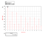
Well, since I got a warning from the inductance I have swapped the model for the regular component but it haven't changed the situation. I tried to remove the oscprobe and use the nodes and It seems that with for F[1]=1GHz and order,harm=15 the oscillator works. Although I got that graf and that table:
View attachment 102813

Shouldn't the first harmonic be the 1GHz signal? I don't understant this. Am I wrong?
Although I got the graf and the table I get the warning: With Order[1]=15 and Harm=15, the oscillator signal has only 1 harmonics. This may not be enough to accurately simulate the oscillator.
So it seems that the simulation is not working properly.

Any other tips?

Ty very much
You make a fundamental error in your setup.
If you intend your oscillator to work at around 850MHz, you should define frequency field in HB controller slightly less than this.For instance 500MHz and 10 harmonics.In HB controller, you should setup seeking range as 3 octaves and 100 or more frequency points ( it's a good to start).So, your HB controller will seek the oscillator frequency from 500MHz to 2000MHz ( 3 octaves).
Also, you should define oscillator nodes being as differential in your case.( e.g.for instance VoutP and VoutN ).
In result page, HB will give you fundamental frequency power/voltage in spectrum by terms of index. not frequency.Frequency can be tabulated in a seperate table.
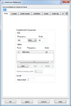
HB_Controller_1.pngHB_Controller_2.pngHB_VCO.pngOutput.png
 
Last edited:
  • Like
Reactions: Coust

    Coust

    Points: 2
    Helpful Answer Positive Rating
You make a fundamental error in your setup.
If you intend your oscillator to work at around 850MHz, you should define frequency field in HB controller slightly less than this.For instance 500MHz and 10 harmonics.In HB controller, you should setup seeking range as 3 octaves and 100 or more frequency points ( it's a good to start).So, your HB controller will seek the oscillator frequency from 500MHz to 2000MHz ( 3 octaves).
Also, you should define oscillator nodes being as differential in your case.( e.g.for instance VoutP and VoutN ).
In result page, HB will give you fundamental frequency power/voltage in spectrum by terms of index. not frequency.Frequency can be tabulated in a seperate table.
View attachment 102815View attachment 102816View attachment 102817View attachment 102818

Ty very much BigBoss!
I have another question for you:
Looking your circuit I saw that you ended our Vout wire with a 50 ohm load. I understand why in Rf circuits we use a 50ohm as a standar but by using this load, are you simulating a connector? I mean, if your Vout signal is going to a SMA connector of 50ohm and then you use a coaxial cable to drive your signal to your oscilloscope, shouldn't you have to use a capacitor in paralel with your load to simulate the parasitic capacitance of your coaxial cable?
I have been checking Rf designs and all of them use only a 50ohm resistor, without any capacitor. What am I missing here?
Why you don't mind about those parasitic elements?

Ty for all your help.
 

Ty very much BigBoss!
I have another question for you:
Looking your circuit I saw that you ended our Vout wire with a 50 ohm load. I understand why in Rf circuits we use a 50ohm as a standar but by using this load, are you simulating a connector? I mean, if your Vout signal is going to a SMA connector of 50ohm and then you use a coaxial cable to drive your signal to your oscilloscope, shouldn't you have to use a capacitor in paralel with your load to simulate the parasitic capacitance of your coaxial cable?
I have been checking Rf designs and all of them use only a 50ohm resistor, without any capacitor. What am I missing here?
Why you don't mind about those parasitic elements?
Ty for all your help.
At that frequency, the parasitic effects ( series resistance,parallel capacitance,series inductance etc.) of the connector-for instance SMA or N-Type-are pretty negligible because those connectors can work up to 26GHz. If you use a 50 Ohm coaxial cable just after this connector, you may extract the attenuation of this cable if you wish measure your circuit precisely.But again, the attenuation of a high quality cable is quite low at those frequencies.Parasitic effects are taken into account when the signal has more than few GHz or if you would like to measure it very precisely.If you consider the load impedance as 50 Ohm, you shouldn't have to modelize your coaxial cable because characteristic impedance of this coaxial cable is almost real.You will see 50Ohm real impedance if you terminate it with a real 50 Ohm ( for instance a measurement equipment) whatever its length is.
Another thing, the oscillators are practically not measured with oscilloscopes, instead Spectrum Analyzer would be the right equipment for you to observe the frequency,its' harmonics,maybe Phase Noise and frequency drifting by temperature etc.Oscilloscopes are time domain equipments and you cannot observe these quantities with it.
 
Ok, I understand it. I was simulating with a 40pF capacitor in paralel with the load because I checked that the best 50ohm cable has 85pF/m and in the lab we use 0.5m coaxial cables. When I simulate with the capacitor, Vpp of Vout2 decrease until reach 50mV instead of 200mV that I get without this parasitic. That's why I was loooking for help in this problem. Do you think that is just a mismaching problem?
Here the pictures with and without the parasitic:
40pF 0.5m.jpg0pF.jpg

Probably the advice here is to get a shorter cable to avoid this capacitance. My advisor said that he have seen the checking of oscillators with the DUT connected directly to the oscilloscope (through a SMA-BNC adapter) to avoid this capacitance. Do you know something about this?

Ty again, I really appreciate this effort.
 

Ok, I understand it. I was simulating with a 40pF capacitor in paralel with the load because I checked that the best 50ohm cable has 85pF/m and in the lab we use 0.5m coaxial cables. When I simulate with the capacitor, Vpp of Vout2 decrease until reach 50mV instead of 200mV that I get without this parasitic. That's why I was loooking for help in this problem. Do you think that is just a mismaching problem?
Here the pictures with and without the parasitic:
View attachment 102948View attachment 102949
You cannot consider the coax cable being as " a lossles cable with a parallel capacitor"..
It's absolutely wrong...
This capacitor is distributed capacitor and it can not be cumulated at one side.
Instead, use measured s-parameters of this cable.It's very easy, calibrate a proper VNA and connect this cable and measure it.Obtain s-parameters in Touchstone format and put these s-parameters in a
"2-ports data Items" block at the output of your oscillator.It will be more accurate..
Also, 200mV output level without parasitic elements is too low for an oscillator.You oscillator is probably wrong polarized or it's loaded too much or Q factor of the tank circuit is not enough.
Look at the output of my oscillator that is almost working at the same frequency below.
If you would prevent it from load components, you have to use a buffer like me.
Output Voltage.png
 
Last edited:
  • Like
Reactions: Coust

    Coust

    Points: 2
    Helpful Answer Positive Rating
Your advice is very helpful, ty very much. I still have a problem with the HB convergence. But the most weird is that if I use an oscport or only the nodes, I get a different kind of error. If I use the oscport at the same point as the first circuit at the top of the page, I get this:

"Warning detected by hpeesofsim in frequency search during HB analysis `HB1'. Circuit is stable. A loopgain with a 0.0 degree phase component was found but the magnitude of the loop gain was less than 1.0 with a clockwise loop gain versus frequency plot trajectory. The loopgain of of the circuit needs to be increased. Will try fixed frequency amplitude search.
Error detected by hpeesofsim in level search during HB analysis `HB1'. Cannot increase oscport level to set loop gain to 1.
Warning detected by hpeesofsim during HB analysis `HB1'. Oscillator analysis did not converge. Setting solution to zero."

On the other hand, if I use the nodes method:

"Warning detected by hpeesofsim in frequency search during HB analysis `HB1'. Circuit is stable. No zero phase crossings of the injected current were found. For oscillation, a negative going zero phase crossing should exist. Will try fixed frequency amplitude search.
Error detected by hpeesofsim in level search during HB analysis `HB1'. Cannot increase oscport level to set injected current to 0.
Warning detected by hpeesofsim during HB analysis `HB1'. Oscillator analysis did not converge. Setting solution to zero."

I played some HB parameters like solver method, robustness, etc. but I didn't improve anything. Is it the oscport properly connected?

Any advice? Or swear...

Ty very much! I will thank you all your effort in my master's thesis! :)

An oscillator has few important parameters which impact the operation of the oscillator.
-Quality Factor of the Tank Circuit including all loading effects.
-Biasing
-Negative Resistance of the Active part so that absolute value should be at least 2.5 times all over parallel equivalent of the passive part including Load,Tank Circuit,Varactor Diodes,other layout parasitics etc.
-Compatibility of the transistors ( some transistors can provide more negative resistance compare to some others at the same biasing condition.)

That's because your oscillator does not work well ( I mentioned before ) or works at very critical point.The output should be more than few hundreds millivolt.
Check first negative resistance, if necessary decrease current or try other transistors.Play around it a bit..
Second, design tank circuit carefully so that parallel equivalent resistance wouldn't exceed that rule of thumb defined above..
And use a proper buffer amplifier to decrease the loading effects.

You can also inspire from my VCO circuit.
 

If you use positive vtune voltage Your Varactor Diodes are wrong polarized
Look at my VCO circuit and put some coupling capacitor between circuit and the diodes.
 
If you use positive vtune voltage Your Varactor Diodes are wrong polarized
Look at my VCO circuit and put some coupling capacitor between circuit and the diodes.

Hello again BigBoss and Ty. I don't get why do you said that the varactors are wrong polarized. If the tank nodes (a,b) oscillate around 1.8V (2.2-1.6), I should be able to polarize them with a 0 to 1.6V vtune in this configuration. Am I wrong? Why do you need those coupling capacitors in the tank? Don't you need a DC signal to reverse polarize the varactors?
I have a couple of questions about your schematic that I would appreciate If you can answer:
HB_VCO.png

What is the function of this elements? Biasing the BJT (resistance and capacitor) and decoupling the DC signal (3.3pF capacitance)?

Finally I'm working with this buffer configuration:

New buffer configuration.jpg

I get a 0.3Vamp signal in the 50ohm load so I find almost a 0dBm power in the load (simulating a differential antenna). What do you think about this circuit? The buffer doesn't amplifier the signal (0.8Vamp before tank and 0.3Vamp in the load). I have tried the emitter follower configuration with the current mirror but the sine wave I got was worst and I don't know how to do maths properly in a diferencial configurations, with a diferencial antenna. Any bibliography or tips?

I know that there are a lot of questions here and it's not your work to solve my problems, but I really appreciate that someone that has knowledge in the matter helps me.

Really, really grateful.
 

Hello again BigBoss and Ty. I don't get why do you said that the varactors are wrong polarized. If the tank nodes (a,b) oscillate around 1.8V (2.2-1.6), I should be able to polarize them with a 0 to 1.6V vtune in this configuration. Am I wrong? Why do you need those coupling capacitors in the tank? Don't you need a DC signal to reverse polarize the varactors?
I have a couple of questions about your schematic that I would appreciate If you can answer:
View attachment 103198

What is the function of this elements? Biasing the BJT (resistance and capacitor) and decoupling the DC signal (3.3pF capacitance)?

Finally I'm working with this buffer configuration:

View attachment 103199

I get a 0.3Vamp signal in the 50ohm load so I find almost a 0dBm power in the load (simulating a differential antenna). What do you think about this circuit? The buffer doesn't amplifier the signal (0.8Vamp before tank and 0.3Vamp in the load). I have tried the emitter follower configuration with the current mirror but the sine wave I got was worst and I don't know how to do maths properly in a diferencial configurations, with a diferencial antenna. Any bibliography or tips?

I know that there are a lot of questions here and it's not your work to solve my problems, but I really appreciate that someone that has knowledge in the matter helps me.

Really, really grateful.
If you use this configuration, the reverse voltage for the varicaps will be limited by supply voltage of the VCO. For instance, if your supply voltage is 1.6V, varicap voltage can not exceed approox. 1.6+0.65V=2.25V due to forward biasing property.If you use capacitor coupled varicaps configuration, you will have more freedom.
Regarding to my circuit..
the RC circuit is used to polarize the buffer from VCO (resistance) and to couple the RF without any attenuation ( capacitor).You can obviously also use a separate bias circuit, no doubt.
Decoupling capacitors (3.3pF) are necessary because I have used a ideal transformer to convert differential-single ended.Capacitors block DC to make the output short circuit.
Buffer amplifier will of course not have a gain because it's an emitter follower ( Collector grounded ).The output voltage will be less than input one by at least Vbe. But in order to drive low impedances and have a current gain, the buffer is necessary.If you would have a large signal swing, you can also use a differential pair by cost of circuit complexity and current consumption.It's up to you..
An improved version looks like that...( I have improved Phase Noise and start-up conditions)
 
  • Like
Reactions: Coust

    Coust

    Points: 2
    Helpful Answer Positive Rating
Ty again, BigBoss. I have another question: Why do you need the current mirror part? I have seen that usually you can use this to double bias the BJT (With VCC from above and with the current source) but you have 3 biasing points (one from the VCO, another from VCC and the last one from the current source), don't you? Do you have some bibliography or book to explain the buffer part?
We usually say that this is a current amplifier but If the voltage gain is a little less than 1 and we fix the load, the current thru the load is fixed too, and it only depends on the voltage of the base, isn't it? So, are we decresing the base current with this? because I don't understand how get a voltage gain equal to 1 and a current gain at the same load. Am I wrong?

Ty very much
A buffer has always a voltage gain smaller than 1.Current gain is the goal here..Therefore in order to drive low impedances a buffer amplifier is a must otherwise the VCO will be loaded a low impedance it will perhaps stop the oscillation in different conditions.In fact there is a single supply here.I have used 2 for simulations only.The current source can be obtained from the same supply.
You can read something about buffer stages in almost all textbooks.
 
  • Like
Reactions: Coust

    Coust

    Points: 2
    Helpful Answer Positive Rating
Ty very much.
Is there any way to find the equivalent resistance of the tank and the active load (bjt) usign ADS? Or do I have to find it analytically?
If analytically, I checked that the bjt differencial pair have a -2gm resistance so if I have Ic=2mA it drives to a -26Ohm resistance. Is it low? I don't know how to check the tank resistance. Do I have to introduce the parasitic resistances of the bjt to the tank?

Thank you!
You can find the negative resistance of the active part by doing a simple s-parameter simulation.
It will be approx. -2/gm but there are some parasitic capacitors and these will change the imaginary part ( not real part) of the active portion.
The procedure is essentially simple but if you look at some sample project files of ADS, you will find lot of useful information about oscillator design and simulation techniques.
Look at especially Closed Loop Transfer Function and its pole-zero specification, it will give you a strong information about your oscillator will work or not.
Read something about the theory of the oscillators.It doesn't make sense to you explain all details here..
 
  • Like
Reactions: Coust

    Coust

    Points: 2
    Helpful Answer Positive Rating
Well BigBoss, I finally have gotten the HB simualtion! At last! The problem was all the time the bottom mosfet bias. The reason is that I want to get an OOK modulation so I need a pulsed Vdc source at the mosfet gate to get those pulses.
When I wanted to test the oscillator alone I only changed the pulse width and its period so I got a sort of common DC source with a little time rise. When I swap that dc pulse for a regular dc source I finally got the HB simulation to work without errors.

Ty very much for all your effort and patience with me and my work.
 
Status
Not open for further replies.

Part and Inventory Search

Welcome to EDABoard.com

Sponsor

Back
Top