Continue to Site

Welcome to EDAboard.com

Welcome to our site! EDAboard.com is an international Electronics Discussion Forum focused on EDA software, circuits, schematics, books, theory, papers, asic, pld, 8051, DSP, Network, RF, Analog Design, PCB, Service Manuals... and a whole lot more! To participate you need to register. Registration is free. Click here to register now.

Problem with CREE SIC CCS050M12CM2 3 phase module with Si8233 Gate Driver as Inverter

Status
Not open for further replies.

powerelectronics_beginner

Newbie level 6
Joined
Aug 24, 2015
Messages
12
Helped
0
Reputation
0
Reaction score
0
Trophy points
1
Activity points
123
Hi guys, we designed a PCB with the formerly mentioned CREE Six-Pack module and 3 pcs. of Si8233 Gate Drivers, one for each phase leg to work as a pure sine wave 50Hz AC inverter. We configured the µC to drive 2 legs in full bridge configuration with filtering inductance and capacitor as well as load resistor between two legs with inverted modulation so that FET 1 and 4 are conducting simultaneously followed by 2 and 3. Software is working fine, we have no control circuit and current measurement in there yet and driving it with the help of a look-up table - 50Hz sine with peak value according to the set DC-link voltage appears on the output clamps correctly.

Now lets get to the problem. Our minimum load is approximately 80Ohms. With this load we are able to increase the DC-link voltage up to 130V, than the 50Hz sine is getting bad caused by faulty gate signals, it starts to break in near its amplitude. The PWM coming from the TI µC board is getting bad as well and starts to oscillate getting below the lower threshold of 0.8V which causes the Si8233 gate signal malfunction. When we decrease the load resistance to 60Ohms this problem is starting earlier at 70V dc-link voltage.
Now we disconnected the coil so that every phase-leg can work without any load and on its own, when DC-link voltage is 0V everything is fine, gate signals are ok. But when we turn up the dc-link voltage and the switching nodes have different voltage levels the problem starts to occur and the PWM signal starts to oscillate even with no load current flowing through the FETs because of the open load circuit. We checked dead-time, gate resistors (tested with 10R,20R,40R) and we soldered ferrite beads to the gate pins like it is recommended by CREE in their circuit for the SIC evaluation board with SI8233 driver as well. We also pull the gate to -5V by using zener diodes for faster turn of like it seems to be common design practice considering example circuits from different manufacturers. The 24V isolated supply voltage for the driver gets supplied by RECOM R2S-0524 isolated DC-DC converters soldered near the drivers which provide us the isolated voltages and grounds for the 6 different gate circuits.

Do you guys have any idea how the gate driver can cause the PWM signal to oscillate? We think that this shouldnt be possible in any way. We also soldered the PWM signal leads directly and as short as possible to the PWM input pins 1 and 2 of the gate driver to mend the potential problem of the long PWM traces inside the PCB.

Maybe someone of you guys can give us a hint on the possible reason for our problem.

Best regards

- - - Updated - - -

circuit.png this is basically our circuit
 

Hi,

to me it seems to be a GND or GND loop problem.

Maybe the load current generates ground bounce between microcontroller and SiC driver.

Try to measure the GND to GND voltage bettween any microcontroler GND pin and pin 4 of SiC driver.

***
I personally don´t like any wire, connection, or anything else in the GND pin connectio of the lower side SiC FET (Picture right bottom corner). Because of the switched high current it should be as low impedance as possible in my eyes. Maybe but not very likely this causes the described problem.

To better analyse the problem we need a picture of the PCB with a description of the high power paths, the signal paths and the GND paths.

Klaus
 
False switching of fast inverters as soon as the DC bus voltage is exceeding a certain level sounds familiar to me. This usually happens if the control circuit picks up output stage switching transients. Can be a ground wiring problem as mentioned by KlausST, but there are many other possibilities. Welcome to the amazing world of fast switching power electronics.

I notice that RECOM R2S DC/DC converter is specified with maximum 110 pF isolation capacitance which is quite a lot. The current transients injected by the high side DC/DC converter can easily bring up effects like you are observing.
 
Hello guys,

thanks a lot for your fast answer and advice Klaus and FvM.
We also noticed that the DC/DC converter are producing humming noises when the problem with the bad PWM signal occurs, its clearly audible when you get your ear to the RECOM R2S but the 24V isolation voltage remains quite steady. Weexperienced this effects at nearly any switching frequency, our target is 200kHz but we tested at 20,40,80 - problem occurs everytime.

KlausSTs hint is very interesting and we will do the measurement tomorrow, i will reply afterwards also with the PCB layout.

Best regards,

there is a mistake in my quickly redrawn schematic, of course the upper gate is not fixed at 24V.
 

I also would appreciate to see a layout photo.

I won't expect that the problem depends primarly on switching frequency, instead it's brought up by the fast output transients.
 

I will post picture of it asap.

Does it make any sense to connect analog and digital ground with inductors like Murata BLM noise suppressors for example?
I read it on stackexchange but there are also many people arguing against it and claiming this solution to be useless and only masking problems. We connected the two grounds with four paralleled 0ohm resistors in one point of the circuit. Can we do this any better?

Best regards
 

Hi,

Inductors in Gnd lines/planes are critical. I personally avoid this.

Instead inductors in supply lines help to reduce transient currents (and also in the return path -GND). This helps to keep the Gnd clean.

Here you have noisy power gnd and a digital logic gnd. While the microcontroller output refers to it's digital gnd, the driver input refers to the power gnd. Now during switching of the power - caused by inductance and resistance between both GND planes - there is a gnd bounce. The reduced input voltage may cause the driver to erroneous switch off.

Klaus
 

How much loop inductance and capacitance on the driver? on the load?
What resonant frequency?

Have you tried near field probe loop ( few cm) to scope to look for emissions?
If you dont have one a short ground clip to tip of a scope probe will work to track a current loop radiating with crosstalk. Then use twisted pair if necessary for long tracks.

WHen measuring voltage anything above 30MHz ignore unless you use proper methods without tip and ground lead using only barrel & pin on 10x or 50 ohm coax terminated at both ends. ( add fraction of 50 IN SERIES to source and 50 Load. IN PARALLEL then calibrate. )
 

Hello,

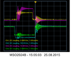
we checked the grounds today, absolutely no bounce on them even with high Vds when the problem gets worst. I attached a waveform of PWM and the according gate signal of high- and lowside FET where the upper graph is the lowside (worse) and the lower graph is the highside. Did someone of you ever see similar curves ?

Best regards

30VnoRC.png
 

Hi,

in your schematic ther are "beads" in the gate lines. Remove them, and see if this brings an improvement.
If the signal is getting worse, then re install them. Try to increase gate drive resistance 20R, 50R and see if this gives an improvement.

The waveform is similar to those with bad pcb layout, especially when the drive path GND is influenced by switched power current, or the .

The SiC Fets - if i remember right - need negative voltage to switch OFF. Did you check datasheet on drive waveform.

How stable is driver supply and bootstrap voltage? Are there high speed ceramic capacitors, with short wide traces to then IC pins?

Klaus
 

I'm guessing that poor isolation in your gate driver supplies it the main culprit. You may need to apply common mode filters to their inputs and/or outputs, or select another isolated converter with less capacitance.
 

Thanks again for replying,
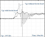
we pull gate to negative 5V for turn-off Klaus. We installed the beads because an application note suggested that they help when having problems in terms of gate control seeing picture attached.
5V driver supply is coming from a bench supply. We already tried different supplies but the phenomenon is occuring unchanged.
Maybe mtwieg is right and we have to focus on the RECOM supplies of the driver. We will try that during the next days.

Best regards

bead.png
 

Using Current probes or 75mV shunts and differential FET probes allows one to compare actual impedances with expected responses from V+ to Gate to drain.
 

The thing is that the gate signal gets disturbed when dc-link voltage exceeds only 5V.

Best regards
 

In this case, should we doubt your measurement setup, circuit wiring or everything?

I see the problem that everybody taking part in the discussion has some expectations how a working gate control circuit should be wired, or how to probe floating circuit nodes. But we don't know how you actually do.
 

Hello guys,

we accomplished to sort out the problem. It was the 24V isolated supply for the high-side running under the Si8233 case and the tracks were located to close to the input side on the left. We saw this issue when we purchased SiLabs demoboards which have the left and right side of the case thoroughly seperated. Cutting the tracks and wiring the IC by hand solved it out. Thanks for all your help !

best regards
 

Status
Not open for further replies.

Similar threads

Part and Inventory Search

Welcome to EDABoard.com

Sponsor

Back
Top