twteng
Junior Member level 1
Hi all:
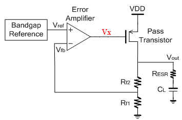
I am designing a LDO as show in attached, Can anybody tell me how to decide the Vx? my spec. of vin range is 2V~5V
regulated output voltage is 1.8V.
Usually, we'll design Vx to vdd/2, but that will enlarge the size of power mos, and induced more parasitic capacitor in the node of Vx,
Can I design the Vx slightly less than vdd/2 to reduce the size of power mos? Does it has any side effect?
Moreover, Does the error amplifier need buffer to drive power mos??
I am glad to hear any suggestions, thanks.
Eason