Continue to Site

Welcome to EDAboard.com

Welcome to our site! EDAboard.com is an international Electronics Discussion Forum focused on EDA software, circuits, schematics, books, theory, papers, asic, pld, 8051, DSP, Network, RF, Analog Design, PCB, Service Manuals... and a whole lot more! To participate you need to register. Registration is free. Click here to register now.

Problem in driving the high side mosfet with L6599( Resonant controller)

Status
Not open for further replies.

tictac

Full Member level 5
Joined
Oct 22, 2006
Messages
297
Helped
3
Reputation
6
Reaction score
3
Trophy points
1,298
Location
Polland
Activity points
3,572
Hi
I want to build the high voltage smps with the output voltage at about 30KV and maximum current= 20mA with L6599

For disabling standby mode I connect pin5 to pin4 .
For disabling current sense I connect pin6 to GND .
VCC(L6599_PIN 12)=15.3 volt , It supplied from one 15volt transformer.

I have a problem for driving high side mosfet(IRFP460 or IRF840) .

The gate resistor is 47 ohm , boot strap capacitor is about 100nF . The wave form of the low side mosfet's gate source is good (50% duty cycle and the clean square wave form- 15volts range) but the wave form of the high side mosfet's gate source is not good( 20% duty cycle, very noisy wave form- 10 volts range) . It makes the high side mosfet get too hot and burned after some minutes( even if it doesnt connect to the high voltage transformer ).

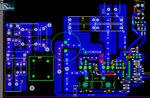
I attach the schematic of my circuit and the wave form of the high side mosfet's gate source.
highside-gate-source.jpg

Please help me for improving high side mosfet's gate source

Regards
Hamed.
 

Attachments

  • highside-gate-source.jpg
    highside-gate-source.jpg
    366.9 KB · Views: 164
Last edited by a moderator:

I can't read that file. Can you post it here in one of the common file formats (pdf or gif for example)?
 

Hi
I attach the schematic and picture of the gate source.
 

Attachments

  • l6599_llc.pdf
    22 KB · Views: 307

Hi
Now I separate the transformer from controller section(L6599) . For closing the feedback loop I put one multi-turn at the intput of the opto-coupler . By changing the resistance of the opto-coupler the frequency changes. I still have the bad driving of the high side mosfet's gate-source. I see some spike about 2.5 volt peak-peak on the below pin :

pin 4 , pin 7 , pin 12 , pin 1

I add some capacitor near the pins(about 100nf to 1uf) . It was a little better and spike on the pin7 get lower range, but they still have a spikes. I think these spikes on the pins cause the problem. I wonder about these spikes although, there is no transformer ,which is connected to the controller circuit.

Regards
 

as i know, st developed improved version of this controller. its 6599A. maybe try to read errata of 6599 to locate the problem?
 
  • Like
Reactions: tictac

    tictac

    Points: 2
    Helpful Answer Positive Rating
  • Like
Reactions: tictac

    tictac

    Points: 2
    Helpful Answer Positive Rating
as i know, st developed improved version of this controller. its 6599A. maybe try to read errata of 6599 to locate the problem?
Thanks you for the important notification about the problems of the L6599. I cant find the errata of L6599. Can you help me for finding this problems list?

- - - Updated - - -

I Connect one diode(BYT43M) from pin 12 to pin 16 for replacing the internal bootstrap diode. The wave form of the high side mosfet gate-source get better. I attach the picture of gate-source. But the mosfet still get too hot without any output transformer. Contrary to the datasheet of the L6599 , the duty cycle of the mosfet's low side and high side is not 50%. Toff=3 uS & Ton=4 uS . Its wonderful .

Its the High side mosfet gate-source
Gate-source_highside.jpg

Its the low side mosfet gate-source
Gate-source_lowside.jpg

For testing and diagnostic of the problem , I disconnect the pin 7 from input voltage divider resistors and I connect this pin to the separate power supply with 3 volt output range . (with common ground ) and I disconnect the input voltage from AC input line(220 vAC) . I see that the high side mosfet gate-source was corrected and it was like the low side mosfet gate-source. The duty cycle of the mosfet's low side and high side still is not 50% and the mosfets dont get warm .
when I connect the input line ac (220 vAC), the waveform of the high side mosfet get noisy and the mosfet get warm.
I think there is a very little dead time between the gate driving of the high-side and low-side of the mosfet and it cause the warming problem.
I dont have access to the L6599A now.
 

Getting textbook waveforms is critical, so use very short probe ground or remove clip and ground lead and only use probe tip and barrel ring.

Learn to use two probes as differential probes using invert Ch2 and add to Ch1. Test CM rejection by probing noisy signal on both probes. If balanced, matched, non-inductive ground leads, you will get a flatline noise free trace. This also teaches you to beware of ground inductance on switched current signals and make your connects, not only low ESR but low ESL.

To monitor cross conduction or shoot thru current, put a 100mV shunt resistor between complementary drivers, tiny , and close between drivers, then use above differential probe measurement to monitor current and correlate with voltage on either side to see how to minimize ringing from shoot-thru. Latency on gate control voltage is a complex RC time response with effective capacitance becoming the greatest during switching. This can be moderated with some dead time by nonlinear RC-diode controls and biasing the gate voltage for rise/fall control to provide 1us of dead time. Approx.
 
  • Like
Reactions: tictac

    tictac

    Points: 2
    Helpful Answer Positive Rating
Thanks for the response.
Can I change the dead time ? As I know we cant change the dead time of the L6599. Can you describe it a little more?

Regards
 

To ask an ignorant question, how do you measure the highside gate source voltage? Do you have a high speed differential probe? Even with it, the waveform you see must not necessarily match the real one.

Regarding spike causes, I would prefer a layout photo to understand about possible grounding issues.
 
  • Like
Reactions: tictac

    tictac

    Points: 2
    Helpful Answer Positive Rating
>>Learn to use two probes as differential probes using invert Ch2 and add to Ch1. Test CM rejection by probing noisy signal on both probes. If balanced, matched, non-inductive ground leads, you will get a flatline noise free trace. This also teaches you to beware of ground inductance on switched current signals and make your connects, not only low ESR but low ESL.>>

My oscilloscope doesnt have inverting and adding mode . But I try to have short tracks for grounds and vdc nets .I try to separate high current ground from low current ground. I attach the picture of the controller pcb for better understanding.
l6599-pcb.jpg

- - - Updated - - -

>>Do you have a high speed differential probe? Even with it, the waveform you see must not necessarily match the real one.>>
Hi
The speed of my probe is 60Mhz. what do you mean of differential probe?

>>how do you measure the highside gate source voltage?>>
I connect the ground lead of the probe to the source of the high side mosfet and the other lead to the gate.

Regards
 

Attachments

  • l6599-pcb.jpg
    l6599-pcb.jpg
    431.5 KB · Views: 174
Last edited:

I have never seen a scope made without Channels that did not have Ch2 invert and Ch1+2 display or A-B. (incredibly useful)

How long are your ground leads? More than a couple cm? Too long. It acts like antenna with inductance. Add test points for signal and ground separated by a few mm and only use probe barrel+ tip. if you still get ringing, it is the inductance and stray or drain capacitance in your load. Use low ESR caps only.
 
  • Like
Reactions: tictac

    tictac

    Points: 2
    Helpful Answer Positive Rating
Thanks for showing the layout. I think there room for better (low inductance) ground wiring around the controller chip, e.g. a ground pour below most of this part of the circuit.

I connect the ground lead of the probe to the source of the high side mosfet and the other lead to the gate.
Did you use a safety transformer for the oscilloscope or the inverter input? In any case, connecting the probe ground to the hot push-pull node will load the circuit with a large parasitic capacitance and disturb the waveforms.

I'm no sure if the two-probe differential measurement will give good results with the high switching voltage present at the high-side source, but it's surely better than the former method.

A differential probe is an external accessory part connected to the oscilloscope. It's a high voltage differential amplifier, usually battery powered.
 
  • Like
Reactions: tictac

    tictac

    Points: 2
    Helpful Answer Positive Rating
Hi--I think our friend problem is not about noisy waveform of the gate signal but also about the duty cycle of the high side gate drive signal--if you consider the first post you can see it.long time ago i had the same problem and couldn't solve it.so if somebody could help; i would be thankful.
 
  • Like
Reactions: tictac

    tictac

    Points: 2
    Helpful Answer Positive Rating
Thanks of all
My main problem is the high side mosfet that getting too hot . I want to improve this problem. Now the voltage range of the mosfet's gate-source is enough for better switching for it . I think I should find the way for reducing the heat.
Please help me for this important problem.
Regards
 

Tictac
Without a sufficient test measurements and full design details, we can only guess.

Is it a problem with excessive thermal resistance? If so, what is power dissipation, temp. rise, heat sink design?

Is it a problem with excessive electrical resistance? If so what is load resistance and MOSFET RdsOn, Voltage current


Without differences from benchmark design or specific measurements separating static and dynamic losses, how can we help? https://www.st.com/web/en/resource/technical/document/application_note/CD00275867.pdf
 
  • Like
Reactions: tictac

    tictac

    Points: 2
    Helpful Answer Positive Rating
Hi SunnySkyguy
I think my problem is excessice electrical resistance. There is no load resistance or no transformer at the mid point of the half bridge.At first I use IRFP460 but because of high Qg and high gate-source current I change it to IRF840.
Input voltage is about 300 volts.
My main problem is the high side mosfet that getting too hot without any load resistance.we know that the at the no-load, the switching frequency get higher and go far away from resonance point and I guess the the efficiency of the converter is getting lower and it causes the thermal problem. I disable standby mode by connecting pin5 to pin4 .
Or maybe insufficient deadtime causes the thermal problem.

Thanks you for the link . But it uses L6599A instead of L6599.

Regards
 

If it was static electrical resistance issue, it would be cold at no load.

Therefore you have a dynamic electrical loss issue, which could be shoot-thru, but you have not recorded the current between hi/lo side, so we can only guess.
 
  • Like
Reactions: tictac

    tictac

    Points: 2
    Helpful Answer Positive Rating
Hi
The DC current of the rectified input voltage(220vAC) is about 60mA .
Recently, I changed L6599 with L6699D. I use one smd to dip converter for connecting new smd resonant controller(L6699D) to the old IC socket(L6599) . After some resistors and capacitors changing, I tested it .
I connect the current measuring circuit to the pin6 of L6699.
I set the maximum , minimum and start-up frequency for the L6699.
I setup the old adjustment due to the start-up requirement of the L6699.
Unfortunately, the both mosfet are still get warm after seconds. :cry:
I think with L6699 the warming problem was resolved .
I connect the transformer to the controller circuit and the output goes up to 8kv.(there is no load at the output) . because of very light load at the output of the transformer(about 60 Mega-ohm) the operation frequency get to 250khz. I think such a high frequency cause the warming problem.

What can I do now?
Regards
 

Hi
Finally, the mosfet warming problem was solved. I think this problem was caused by the L6599 and they resolve it by producing the newer generation of resonant controller(L6699).
I set the maximum frequency to 200khz and F-start=190khz and F-min=60khz . CF=330pf( due to table6 of L6699 datasheet )
Resonance capacitor=110nF
Ls(series inductance)=94 uH
Lp(parallel inductance)=250 uH
I set the C40=120 pF , R18=40 ohm

For testing I connect one multi-turn (100k) at the input of the opto-coupler and by changing the resistance the output voltage must changes from 2volt to 0 volt and it cause the changing of frequency. But because of incorrect sensing of the current at pin6 the frequency doesnt reduce.(because of common mode noise on the all input pins) The output voltage almost was fixed(about 10kv) . I want to change to 30kv by reducing the operation frequency.

I have a loud spike on the current sense line that causes the incorrect sense of actual current of the network. How can I reduce the spike?
I attached the new schematic with last changing for l6699.

Regards.
 

Attachments

  • llc.pdf
    21.1 KB · Views: 215

Status
Not open for further replies.

Similar threads

Part and Inventory Search

Welcome to EDABoard.com

Sponsor

Back
Top