Continue to Site

Welcome to EDAboard.com

Welcome to our site! EDAboard.com is an international Electronics Discussion Forum focused on EDA software, circuits, schematics, books, theory, papers, asic, pld, 8051, DSP, Network, RF, Analog Design, PCB, Service Manuals... and a whole lot more! To participate you need to register. Registration is free. Click here to register now.

Problem in Cadence layout

immajidjafari

Newbie
Newbie level 2
Joined
Jul 4, 2019
Messages
2
Helped
0
Reputation
0
Reaction score
0
Trophy points
1
Activity points
12
Hello everyone!
I'm trying to design an inverter layout in cadence but when I import a nmos that's the wrong layout with a white box. and Pmos has the correct layout. This is a screenshot from nmos and pmos beside together. tnx
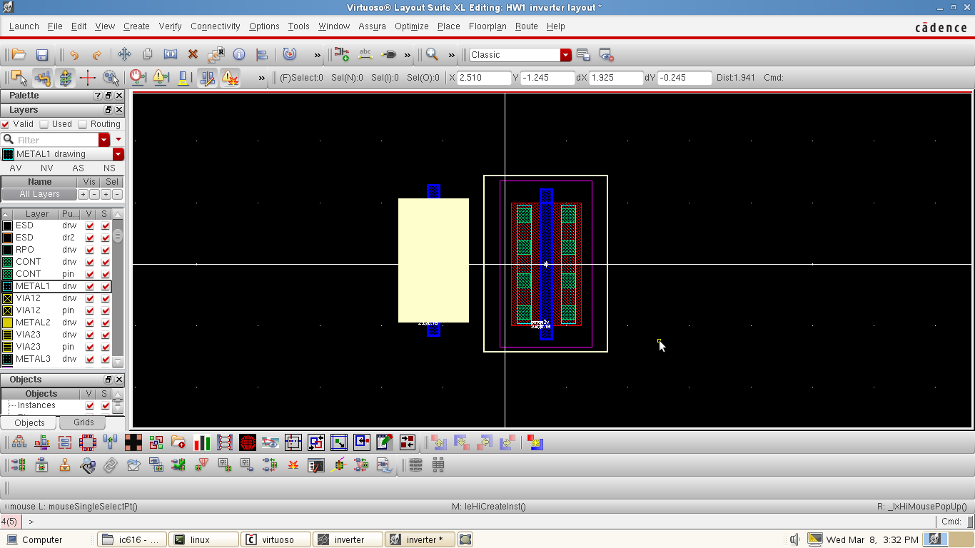

1678307570399.png
 

dick_freebird

Advanced Member level 7
Joined
Mar 4, 2008
Messages
8,244
Helped
2,293
Reputation
4,596
Reaction score
2,334
Trophy points
1,393
Location
USA
Activity points
65,957
Might be just an undesirable fill code on one of the NMOS-specific layers. Go look in the LSW for that kind of solid fill and modify to suit?
 

LaTeX Commands Quick-Menu:

Part and Inventory Search

Welcome to EDABoard.com

Sponsor

Top