Continue to Site

Welcome to EDAboard.com

Welcome to our site! EDAboard.com is an international Electronics Discussion Forum focused on EDA software, circuits, schematics, books, theory, papers, asic, pld, 8051, DSP, Network, RF, Analog Design, PCB, Service Manuals... and a whole lot more! To participate you need to register. Registration is free. Click here to register now.

Problem in Assura LVS with IBM cms9flp

Status
Not open for further replies.

shahriar22nd

Member level 2
Joined
Sep 24, 2009
Messages
45
Helped
0
Reputation
0
Reaction score
0
Trophy points
1,286
Location
Dhaka, Bangladesh
Activity points
1,663
Hellow,
Could anyone please tell me whether it will be possible to do Assura LVS with IBM cms9flp? It's help docs state that, Assura LVS needs two additional files exclusively- IBM_PDK/cms9flp/V1.2.0.0/cdslib/cms9flp/subcircuit.cdl.assura and IBM_PDK/cms9flp/V1.2.0.0/utils/assura_cdl_processor.pl for generating Assura specific CDL netlist and for CDL-processing respectively. But I see, none of these files are present in the PDK.
Anyone please tell me how to proceed for Assura LVS without these files. Are these files essential for the job?

Thank you.
 

You can do DRC (VLDB) with the following settings:

Schematic Design Source: DFII
Library: your library
Cell: your cell
View: schematic

layout is the same configuration but View is layout.
 
Thank you Oermens for your reply. I was trying only for lvs (cdl), because help docs of the pdk speaks a lot about cdl, nothing much about vldb.
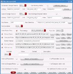
However, I see I have to fill up the LVS form like the attached Fig. Would you please tell me what is to set in the 'Netlisting Options ...' (top-right of the attached Fig) of the LVS form?
Thank you ...
 

i wont be in my office until the 2nd week of jan, but i dont remember ever changing anything in that menu.
 
Ok then. I shall try it tomorrow with default settings except my schematic and layout cell information and shall write here whatever comes out.

One more question please. I learnt that, RF devices have inherent substrate connection and will not pass lvs if any substrate contact like 'subc' is used there explicitly. Situation is just opposite in case of standard devices. Now, for example if I design an amplifier consisting of RF NFETs and biased by a current mirror comprised of standard NFETs, then to pass the lvs, do I have to use a 'subc' explicitly in my cell or not?
Thank you.
 

I could run lvs (vldb). But, I had to generate the cdl netlist and had to process it for lvs before adding it to the assura lvs window ...
 

Could you please give a precise step by step description for the solution of this problem with VLDB LVS & RF Transistors & this damn subc??I am stuck on this over a month and i can't find answer from anywhere...neither from my colleagues nor from IBM's support...

Thanks in advance.I would appreciate any helpful feedback.
 

shahriar22nd or somebody else that has a solution for this???It is very important to me for a fast solution and IBM's technical support team doesn't seem to cooperate for a solution...Let me be more specific with my problem.

I had created a simple test case with nfet_rf from rf9flp library that consists of a single nfet_rf and no subc in the schematic.In addition i removed the default guard ring of the nfet_rf.At the layout side i have the transistor and a subc component.This case passes VLDB LVS and according to IBM's team it is ok and they are working on a solution after my report to them.

Now,let's see the design.It consists of various nfet_rf (only this type of transistor and nothing else like capacitors,regular fets etc...).At the schematic side i use subc (same results if i don't use it since IBM admitted that it causes problem if it exists) and i have removed the default guard ring with substrate contacts of all fets because i create a custom one for all the nmos area in the layout.
Then i run VLDB LVS and i will show you the errors (rewires,nets) i get from LVS at the screenshot below.I also show the setup of the LVS form and all the LVS.cls file.If anymore info are needed for a conclusion i will provide them.

Thanks a lot in advance.I will appreciate any helpful feedback since it is very critical issue for me.
 

Attachments

  • LVS_cls_file.txt
    6.8 KB · Views: 53
  • image_1.jpg
    image_1.jpg
    189.3 KB · Views: 112
  • image_2.jpg
    image_2.jpg
    168.9 KB · Views: 117
  • LVS_setup.jpg
    LVS_setup.jpg
    151.2 KB · Views: 119

hi dear..
could you give me the download linke about IBM PDK?
 

Status
Not open for further replies.

Part and Inventory Search

Welcome to EDABoard.com

Sponsor

Back
Top