Continue to Site

Welcome to EDAboard.com

Welcome to our site! EDAboard.com is an international Electronics Discussion Forum focused on EDA software, circuits, schematics, books, theory, papers, asic, pld, 8051, DSP, Network, RF, Analog Design, PCB, Service Manuals... and a whole lot more! To participate you need to register. Registration is free. Click here to register now.

problem creating pmos caracteristics using spice model LTSPICE

Status
Not open for further replies.

yefj

Advanced Member level 4
Joined
Sep 12, 2019
Messages
1,190
Helped
1
Reputation
2
Reaction score
3
Trophy points
38
Activity points
7,181
Hello, I have tried to implement the PMOS characteristics using the model shown in the link.
I have built the model as shown in the photo bellow.
Vs=1.8V
V_SG=Vs-Vg=1.8-Vg>|Vt| => 1.8-Vg>0.39
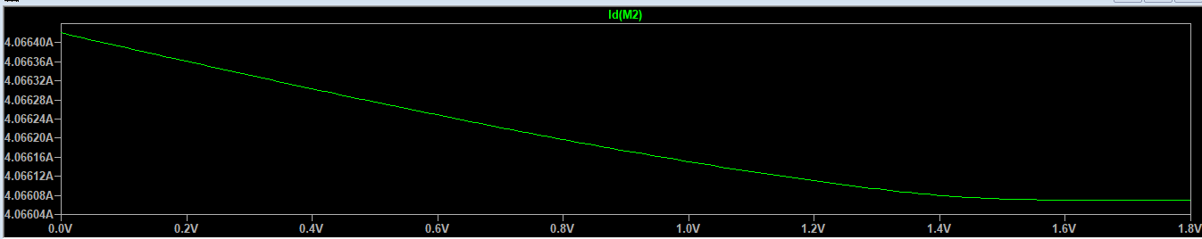
i did a sweep on Vg from 0 till 1.8 so VSG is smaller then 0.39 at some point ,but in reality get the same current on the plot bellow.
Where did i go wrong?
from the manual shown bellow:
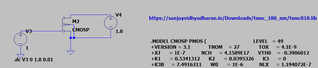
1676491484027.png


VsPrkXvG5dwciMYLf_JHJ4GGlRh0eF3xl_AKaxzADCRKBfWboFsV3TJEQr2MGqif5WcGafPRR48K5mJeBxkCRYru-i-dLAjtigYjel1xi7er9YU86nYXVgXoMvT2WY73xGMo_qKMG0SQtl415PFz_7U

ACq0rdERGfMgSpOm3HnboemG_7NJDD61ZU0neJO3gx9nM1f_3Tw7MwLfyvyyMdNwojhilsp3PC7zbkfx6Edq-H22OzGVVjppD9IfoNk8zHEE27iJq7vP1TkK--YqKcvyi6GhUK-exAlAscXHgPgep7I
 

Where did i go wrong?
A couple of places:

For a P-MOSFET, both voltages must be negative going.
The current your simulation shows is through the substrate parasitic diode (note the direction of the diode arrow).

And if you want a set of characteristic curves, as shown in the reference manual, you need to sweep both voltage sources, as shown in the example below:
Generally you want the gate voltage to start the sweep at the MOSFETs Vgs(ths) (which is -3.2V for the transistor below).


1676496187030.png
 
Last edited:

Status
Not open for further replies.

Part and Inventory Search

Welcome to EDABoard.com

Sponsor

Back
Top